
Texas Instruments
INA126UA
OP Amps, Buffer Amps ICs
INA126UA
687-INA126UA

Texas Instruments-INA126UA-datasheets-3050658.pdf
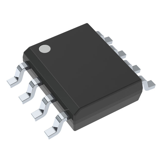
IC INST AMP 1 CIRCUIT 8SOIC


.png?x-oss-process=image/format,webp/resize,p_30)


INA126UA Description
The INA126UA is a high-side current shunt monitor from Texas Instruments. It is designed to measure the current flowing through a high-side shunt resistor with high accuracy and low power consumption.
Description:
The INA126UA is available in a small 10-pin WSON package and operates from a supply voltage range of 2.7V to 5.5V. It features a low-drift, low-offset current shunt amplifier with a gain of up to 40,000. The device also includes a 12-bit ADC with a programmable gain, allowing for a wide input voltage range and high resolution.
Features:
- High accuracy and low drift current shunt amplifier
- Wide supply voltage range: 2.7V to 5.5V
- Low power consumption: 190µA typical
- 12-bit ADC with programmable gain
- Wide input voltage range: up to 56V
- High resolution: 0.2mV
- Small 10-pin WSON package
Applications:
The INA126UA is suitable for a wide range of applications that require high-accuracy current monitoring, including:
- Battery monitoring systems
- Power supplies and energy harvesting systems
- Motor control and management systems
- Solar panel monitoring
- Electric vehicle charging systems
- Portable electronic devices
Overall, the INA126UA is a versatile and accurate current shunt monitor that can be used in a variety of applications where precise current measurement is required.
Tech Specifications
Number of Channels per Chip
Unit Weight
Power Supply Type
Maximum Supply Voltage Range (V)
Dual Supply Voltage
Product
PPAP
Automotive
RoHS
CMRR (min) (dB)
Input bias current (±) (max) (nA)
Gain Error
Voltage gain (min) (V/V)
REACH Status
Maximum Operating Supply Voltage (V)
Input common mode headroom (to negative supply) (typ) (V)
Operating temperature range (°C)
PSRR - Power Supply Rejection Ratio
Gain V/V
Supplier Temperature Grade
Voltage gain (max) (V/V)
Current - Supply
Output swing headroom (to negative supply) (typ) (V)
Standard Package Name
Mounting
Minimum Single Supply Voltage (V)
Moisture Sensitive
Maximum Input Resistance
Package
Minimum CMRR (dB)
3 dB Bandwidth
en - Input Voltage Noise Density
Output Type
Vos - Input Offset Voltage
Vs (min) (V)
Minimum CMRR Range (dB)
Iq (typ) (mA)
Package Height
Maximum Operating Temperature
Ib - Input Bias Current
INL - Integral Nonlinearity
Noise at 0.1 Hz to 10 Hz (typ) (µVPP)
Width
RoHS Status
Number of channels
-3db Bandwidth
Minimum Operating Temperature
Voltage - Input Offset
Type
Input offset (±) (max) (µV)
Length
Operating Supply Voltage
Maximum Voltage Gain Range (dB)
Part Status
Vs (max) (V)
Lead finish / Ball material
Number of Circuits
Package Width
GBP - Gain Bandwidth Product
Voltage - Supply Span (Max)
Maximum Input Offset Voltage (mV)
Maximum Voltage Gain (dB)
Input offset drift (±) (max) (µV/°C)
Product Status
Current - Input Bias
Supplier Package
Package / Case
Number of Channels
EU RoHS
Carrier
Amplifier Type
Maximum Dual Supply Voltage (V)
Input common mode headroom (to positive supply) (typ) (V)
Moisture Sensitivity Level (MSL)
Operating Temperature
Output swing headroom (to positive supply) (typ) (V)
Gain error (±) (max) (%)
ECCN
MSL rating / Peak reflow
Mounting Type
Pin Count
Gain nonlinearity (±) (max) (%)
Minimum PSRR (dB)
Typical Dual Supply Voltage (V)
Voltage - Supply Span (Min)
Lead Shape
HTSUS
Maximum Input Resistance (MOhm)
Pins
Current - Output / Channel
USHTS
PCB changed
HTS
Rating
ECCN (US)
Bandwidth at min gain (typ) (MHz)
Supplier Device Package
Supply Voltage - Min
Minimum Operating Temperature (°C)
Maximum Operating Temperature (°C)
Operating Supply Current
SR - Slew Rate
Mfr
Height
Features
Supply Voltage - Max
Mounting Style
Typical Single Supply Voltage (V)
Maximum Input Bias Current (uA)
Slew Rate
Package Length
Minimum Dual Supply Voltage (V)
CMRR - Common Mode Rejection Ratio
Noise at 1 kHz (typ) (nV√Hz)
REACH
Series
Maximum Single Supply Voltage (V)
Base Product Number
INA126UA Documents
Download datasheets and manufacturer documentation for INA126UA
 Mechanical Outline Drawing
  Product Change Notification (PDF) Product Change Notification 2024-06-28 (PDF)
  INA126UA Symbol & Footprint by SnapMagic
  Comprehensive Error Calculation for Instrumentation Amplifiers
  INA126 TINA-TI Reference Design (Rev. B)
  INA126 TINA-TI Spice Model (Rev. A) INA126 PSpice Model (Rev. A)
 Shopping Guide

Payment Methods
Payment Methods include Prepayment TT (bank transfer), Western Union, and PayPal. Customers are responsible for shipping costs, bank charges, customs duties and taxes.


Shipping Rate
Shipments are made once a day around 5pm, excluding Sundays. Once shipped, the estimated delivery time is usually 5-7 business days, depending on the courier you choose.

Delivery Methods
Provide DHL, FedEx, UPS, EMS, SF Express and Registered Airmail International Delivery Service


.png?x-oss-process=image/format,webp/resize,h_32)


