
Texas Instruments
INA240A4QPWRQ1
OP Amps, Buffer Amps ICs


.png?x-oss-process=image/format,webp/resize,p_30)


INA240A4QPWRQ1 Description
The INA240A4QPWRQ1 is a high-accuracy, low-dropout, micropower shunt and bus monitor from Texas Instruments. It is designed to measure both shunt voltage and bus voltage with high accuracy and low power consumption, making it ideal for battery-powered applications and other systems where power efficiency is critical.
Description:
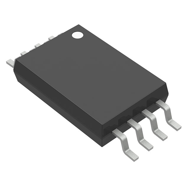
The INA240A4QPWRQ1 is a monolithic, precision current and power monitor that integrates a precision shunt amplifier, a precision bus amplifier, and a 12-bit ADC. It is available in a compact, thermally enhanced, 10-lead WSON package.
Features:
- High accuracy: The INA240A4QPWRQ1 offers high accuracy and low drift, with a maximum current measurement error of ±0.25% and a maximum bus voltage measurement error of ±0.5%.
- Low power consumption: The device operates with a low power consumption of 175µA in normal mode and 2.5µA in shutdown mode, making it ideal for battery-powered applications.
- Wide input voltage range: The INA240A4QPWRQ1 can operate from a wide input voltage range of 2.5V to 5.5V, making it suitable for a variety of applications.
- Programmable gain: The device features a programmable gain amplifier (PGA) that allows for flexible shunt voltage measurement, with gains of 20, 40, 80, or 160.
- Wide shunt voltage range: The INA240A4QPWRQ1 can measure shunt voltages from 10µV to 2.112V, making it suitable for a wide range of applications.
- I2C digital interface: The device features an I2C digital interface, allowing for easy integration with microcontrollers and other digital systems.
- Small package: The INA240A4QPWRQ1 is available in a compact, thermally enhanced, 10-lead WSON package.
Applications:
The INA240A4QPWRQ1 is suitable for a variety of applications where high accuracy and low power consumption are important, including:
- Battery-powered systems
- Portable electronics
- Energy harvesting systems
- Power supplies and power management systems
- Industrial control systems
- Medical equipment
- Automotive systems
- Renewable energy systems
In summary, the INA240A4QPWRQ1 is a high-accuracy, low-dropout, micropower shunt and bus monitor from Texas Instruments that offers a wide input voltage range, programmable gain, and a small package size. It is ideal for a variety of applications where power efficiency and accuracy are critical, including battery-powered systems, energy harvesting systems, and industrial control systems.
Tech Specifications
INA240A4QPWRQ1 Documents
Download datasheets and manufacturer documentation for INA240A4QPWRQ1
 Wafer Fab 23/Dec/2021
  INA240-Q1 Datasheet
  INA240-Q1 Datasheet
  Mult Dev Marking Chgs 16/Mar/2023
 Shopping Guide


.png?x-oss-process=image/format,webp/resize,h_32)


