
Texas Instruments
JM38510/07101BDA
Flip Flops


.png?x-oss-process=image/format,webp/resize,p_30)


JM38510/07101BDA Description
JM38510/07101BDA Description
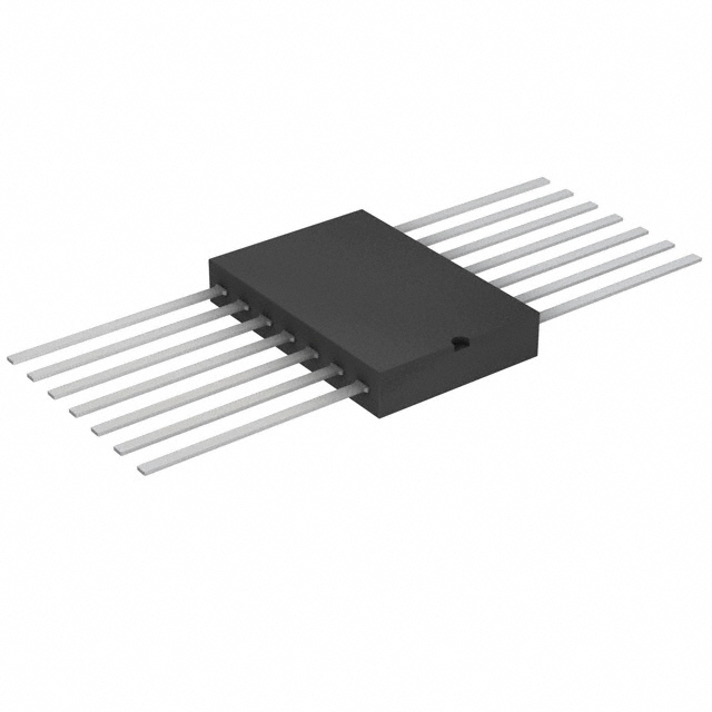
The JM38510/07101BDA is a high-performance dual D-type positive-edge-triggered flip-flop designed by Texas Instruments. This device is part of the 54S series and is optimized for a wide range of digital applications requiring reliable and efficient data storage and transfer. The flip-flop operates with a clock frequency of 110 MHz, ensuring fast and accurate data processing. It features a maximum propagation delay of 13.5ns at 5V and a maximum load capacitance of 15pF, making it suitable for high-speed digital circuits.
The JM38510/07101BDA is designed with a quiescent current of 25 mA, which helps in reducing power consumption while maintaining high performance. Each flip-flop element can store 1 bit of data and provides complementary outputs, enhancing the flexibility of the device in various digital systems. The flip-flop is triggered on the positive edge of the clock signal, ensuring precise timing control.
This device is available in a surface-mount package, making it ideal for modern printed circuit board (PCB) designs that require compact and reliable components. The supply voltage range of 4.5V to 5.5V ensures compatibility with a variety of power supply systems. The output current capability of 1mA for high and 20mA for low states further enhances its versatility in driving different types of loads.
JM38510/07101BDA Features
- High-Speed Operation: With a clock frequency of 110 MHz, the JM38510/07101BDA ensures rapid data processing, making it suitable for high-speed digital applications.
- Low Propagation Delay: The maximum propagation delay of 13.5ns at 5V and 15pF ensures minimal latency in data transfer, crucial for time-sensitive applications.
- Low Power Consumption: The quiescent current of 25 mA helps in reducing power consumption, making it ideal for energy-efficient designs.
- Dual Elements: Each flip-flop element can store 1 bit of data, providing dual storage capabilities in a single package.
- Complementary Outputs: The complementary output type enhances the flexibility of the device in various digital systems.
- Positive Edge Triggering: The positive edge triggering ensures precise timing control, essential for synchronous digital circuits.
- Wide Supply Voltage Range: The supply voltage range of 4.5V to 5.5V ensures compatibility with a variety of power supply systems.
- Surface-Mount Packaging: The surface-mount package is ideal for modern PCB designs, offering compact and reliable mounting options.
- ROHS3 Compliant: The device meets the stringent environmental standards of ROHS3, ensuring compliance with global regulations.
JM38510/07101BDA Applications
The JM38510/07101BDA is ideal for a wide range of digital applications, including but not limited to:
- Digital Signal Processing: The high-speed operation and low propagation delay make it suitable for processing digital signals in real-time.
- Data Storage and Transfer: The dual D-type flip-flops provide reliable data storage and transfer capabilities, essential for digital systems.
- Clock Management: The positive edge triggering and complementary outputs make it ideal for clock management and synchronization in digital circuits.
- Communication Systems: The device's high-speed performance and low power consumption make it suitable for communication systems requiring efficient data handling.
- Control Systems: The dual flip-flops can be used in control systems for storing and transferring control signals, ensuring precise operation.
Conclusion of JM38510/07101BDA
The JM38510/07101BDA from Texas Instruments is a versatile and high-performance dual D-type positive-edge-triggered flip-flop that offers significant advantages over similar models. Its high-speed operation, low propagation delay, and low power consumption make it ideal for a wide range of digital applications. The complementary outputs and positive edge triggering ensure precise timing control and flexibility in digital systems. The surface-mount package and ROHS3 compliance further enhance its suitability for modern PCB designs and environmental standards. Whether used in digital signal processing, data storage, clock management, communication systems, or control systems, the JM38510/07101BDA provides reliable and efficient performance, making it a valuable component in the electronics industry.
Tech Specifications
JM38510/07101BDA Documents
Download datasheets and manufacturer documentation for JM38510/07101BDA
 SN54(74)74, SN54(74)LS74A, SN54(74)S74
 Shopping Guide


.png?x-oss-process=image/format,webp/resize,h_32)


