
Texas Instruments
LF353D
OP Amps, Buffer Amps ICs


.png?x-oss-process=image/format,webp/resize,p_30)


LF353D Description
LF353D Description
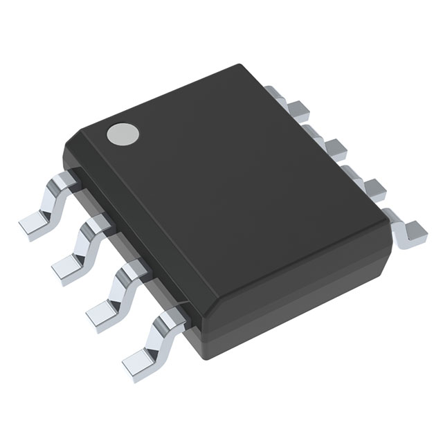
The LF353D is a high-performance, dual-channel operational amplifier (op-amp) from Texas Instruments, designed for precision analog signal processing applications. This IC features a JFET input stage, offering excellent performance characteristics such as low input bias current and high input impedance. The LF353D is housed in an 8-pin SOIC package, making it suitable for surface-mount applications. Despite being marked as obsolete, the LF353D remains a reliable choice for engineers and designers seeking a robust and versatile op-amp solution.
LF353D Features
- Supply Voltage Range: The LF353D operates over a wide supply voltage range from 7V to 36V, providing flexibility in power supply design.
- Gain Bandwidth Product: With a gain bandwidth product of 3MHz, the LF353D delivers high-frequency performance suitable for a variety of analog applications.
- Low Input Bias Current: The low input bias current of 50pA ensures minimal loading on the input signal source, making it ideal for high-impedance circuits.
- High Slew Rate: The 13V/µs slew rate allows the LF353D to handle fast-changing signals with minimal distortion.
- Low Input Offset Voltage: The input offset voltage of 5mV ensures accurate signal amplification and reduces the need for calibration.
- Dual Channel Design: The LF353D features two independent op-amp channels, each capable of sourcing or sinking up to 40mA, providing flexibility in circuit design.
- Compliance and Packaging: The LF353D is REACH unaffected and ROHS3 compliant, ensuring it meets environmental and regulatory standards. It is packaged in a tube, which is suitable for automated assembly processes.
LF353D Applications
The LF353D is well-suited for a range of applications due to its high performance and versatility. Some specific use cases include:
- Signal Conditioning: The LF353D can be used to amplify and condition low-level signals from sensors, ensuring accurate and reliable data acquisition.
- Audio Amplification: Its high slew rate and wide bandwidth make it suitable for audio applications, providing clear and distortion-free sound reproduction.
- Precision Measurement: The low input bias current and offset voltage are beneficial for precision measurement circuits, such as those used in scientific instruments.
- Active Filters: The LF353D can be employed in active filter designs to achieve precise frequency response characteristics.
- Voltage Followers: The dual-channel design allows for the creation of voltage followers or buffer circuits, which can drive high-capacitance loads without signal degradation.
Conclusion of LF353D
The LF353D from Texas Instruments is a high-performance dual-channel operational amplifier that offers a combination of high input impedance, low input bias current, and a wide supply voltage range. Its 3MHz gain bandwidth product and 13V/µs slew rate make it suitable for a variety of high-frequency and precision applications. Despite being marked as obsolete, the LF353D remains a reliable choice for engineers and designers who require a robust and versatile op-amp. Its compliance with REACH and ROHS3 standards ensures it meets environmental and regulatory requirements, making it a responsible choice for modern electronics design.
Tech Specifications
LF353D Documents
Download datasheets and manufacturer documentation for LF353D
 LF353
LF353  LF353x/TL07x/TL08x obs 26/Jul/2022
  LF353
LF353  Mult Devices Font 21/Apr/2018 Design 25/Feb/2022
 Shopping Guide


.png?x-oss-process=image/format,webp/resize,h_32)


