Texas Instruments_LM324BIPWR

Texas Instruments
LM324BIPWR  
OP Amps, Buffer Amps ICs

Texas Instruments
LM324BIPWR
687-LM324BIPWR
Ersa
Texas Instruments-LM324BIPWR-datasheets-3966858.pdf
QUAD, 36-V, 1.2-MHZ, 3-MV OFFSET
In Stock : 10919

Not available to buy online? Want the lower wholesale price? Please Send RFQ to get best price, we will respond immediately

QUICK RFQ
ADD TO RFQ LIST
ersa FreeSample ersa flow
  • Quantity
  • Unit Price
  • Ext. Price
    • 5+
    • $0.15439
    • $0.77
    • 50+
    • $0.12460
    • $6.23
    • 150+
    • $0.11183
    • $16.77
    • 500+
    • $0.09590
    • $47.95
    • 3000+
    • $0.08879
    • $266.37
    ADD TO CART
    QUICK ORDER
    $0.00000    $0.00
    ISO9001
    Quality Policy
    ISO45001
    ISO14001

    LM324BIPWR Description

    The LM324BIPWR is a quad operational amplifier (op-amp) integrated circuit (IC) manufactured by Texas Instruments. It is a low-cost, high-performance device that is commonly used in a wide range of applications due to its versatility and reliability.

    Description:

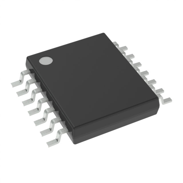
    The LM324BIPWR is a 14-pin DIP (Dual In-line Package) IC that contains four independent op-amps. Each op-amp has a high input impedance, low output impedance, and a wide range of supply voltages (typically ±3V to ±32V). The IC is designed to operate over a temperature range of -40°C to +125°C.

    Features:

    1. Quad op-amps in a single package: The LM324BIPWR contains four independent op-amps, making it suitable for applications that require multiple amplification stages.
    2. Wide supply voltage range: The device can operate with supply voltages ranging from ±3V to ±32V, making it suitable for various power supply configurations.
    3. High input impedance: The LM324BIPWR has a high input impedance, which means it draws very little current from the input signal source.
    4. Low output impedance: The low output impedance ensures that the output signal can drive low-impedance loads without significant voltage drop.
    5. Short-circuit protection: The IC features internal protection against short-circuit conditions, which can help prevent damage to the device in case of a fault.
    6. Low power consumption: The LM324BIPWR has a low power consumption, making it suitable for battery-powered applications.
    7. Wide temperature range: The device is designed to operate over a wide temperature range, making it suitable for use in various environments.

    Applications:

    1. Audio amplifiers: The LM324BIPWR can be used to build audio amplifiers for applications such as headphones, speakers, and sound systems.
    2. Signal conditioning: The IC can be used for amplifying, filtering, or buffering signals in various electronic systems.
    3. Instrumentation amplifiers: The LM324BIPWR can be used to create instrumentation amplifiers for precise measurements in medical and industrial applications.
    4. Active filters: The device can be used to design active filters such as low-pass, high-pass, band-pass, and band-stop filters.
    5. Oscillators: The LM324BIPWR can be used to build various types of oscillators, including sine wave, square wave, and triangular wave oscillators.
    6. Motor control: The IC can be used in motor control applications, such as driving stepper motors or controlling the speed of DC motors.
    7. Voltage regulators: The LM324BIPWR can be used to design voltage regulators for stabilizing and regulating power supply voltages.

    In summary, the LM324BIPWR is a versatile and reliable quad op-amp IC that offers a wide range of features, making it suitable for various applications in the fields of audio, signal processing, instrumentation, and control systems.

    Tech Specifications

    Number of Channels per Chip
    Power Supply Type
    Typical Output Current (mA)
    Rail-to-rail
    Product
    PPAP
    Gain Bandwidth Product
    Automotive
    Maximum Input Offset Current (uA)
    RoHS
    REACH Status
    Input common mode headroom (to negative supply) (typ) (V)
    Operating temperature range (°C)
    PSRR - Power Supply Rejection Ratio
    Current - Supply
    Output swing headroom (to negative supply) (typ) (V)
    Standard Package Name
    Shut Down Support
    Mounting
    Minimum Single Supply Voltage (V)
    Iout (typ) (A)
    Manufacturer Type
    Package
    Minimum CMRR (dB)
    Total supply voltage (+5 V = 5, ±5 V = 10) (max) (V)
    GBW (typ) (MHz)
    Output Type
    Vos - Input Offset Voltage
    Minimum CMRR Range (dB)
    Typical Gain Bandwidth Product (MHz)
    Package Height
    Maximum Operating Temperature
    Ib - Input Bias Current
    RoHS Status
    Number of channels
    Iq per channel (typ) (mA)
    Minimum Operating Temperature
    Voltage - Input Offset
    Type
    Vos (offset voltage at 25°C) (max) (mV)
    Output Current per Channel
    Part Status
    Lead finish / Ball material
    Number of Circuits
    Package Width
    Voltage - Supply Span (Max)
    Maximum Input Offset Voltage (mV)
    Product Status
    Current - Input Bias
    Supplier Package
    Package / Case
    Number of Channels
    Typical Voltage Gain (dB)
    EU RoHS
    Carrier
    Amplifier Type
    Maximum Dual Supply Voltage (V)
    Input common mode headroom (to positive supply) (typ) (V)
    Moisture Sensitivity Level (MSL)
    Typical Input Noise Voltage Density (nV/rtHz)
    Operating Temperature
    Architecture
    Typical Slew Rate (V/us)
    Output swing headroom (to positive supply) (typ) (V)
    ECCN
    MSL rating / Peak reflow
    Mounting Type
    Pin Count
    Ios - Input Offset Current
    Minimum PSRR (dB)
    Shutdown
    Typical Dual Supply Voltage (V)
    Voltage - Supply Span (Min)
    HTSUS
    Pins
    Current - Output / Channel
    USHTS
    PCB changed
    HTS
    Rating
    ECCN (US)
    Total supply voltage (+5 V = 5, ±5 V = 10) (min) (V)
    Supplier Device Package
    Supply Voltage - Min
    Minimum Operating Temperature (°C)
    Maximum Operating Temperature (°C)
    SR - Slew Rate
    Mfr
    Features
    CMRR (typ) (dB)
    Supply Voltage - Max
    Offset drift (typ) (µV/°C)
    Mounting Style
    Maximum Input Bias Current (uA)
    Slew Rate
    Package Length
    Minimum Dual Supply Voltage (V)
    Vn at 1 kHz (typ) (nV√Hz)
    CMRR - Common Mode Rejection Ratio
    REACH
    Series
    Maximum Single Supply Voltage (V)
    Slew rate (typ) (V/µs)
    Typical Settling Time (ns)
    Input bias current (max) (pA)

    LM324BIPWR Documents

    Download datasheets and manufacturer documentation for LM324BIPWR

    Ersa LMx24, LM2902      
    Ersa Device Symbolization Change 13/Jun/2023      

    Shopping Guide

    Payment Methods
    Payment Methods include Prepayment TT (bank transfer), Western Union, and PayPal. Customers are responsible for shipping costs, bank charges, customs duties and taxes.
    Shipping Rate
    Shipments are made once a day around 5pm, excluding Sundays. Once shipped, the estimated delivery time is usually 5-7 business days, depending on the courier you choose.
    Delivery Methods
    Provide DHL, FedEx, UPS, EMS, SF Express and Registered Airmail International Delivery Service