
Texas Instruments
TLC2652AMFKB
OP Amps, Buffer Amps ICs


.png?x-oss-process=image/format,webp/resize,p_30)


TLC2652AMFKB Description
TLC2652AMFKB Description
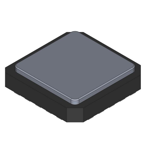
The TLC2652AMFKB is a high-performance, zero-drift operational amplifier from Texas Instruments, designed for precision applications requiring low input offset voltage and high gain bandwidth. This Linear IC Chip is part of the LinCMOS™ series and features a wide supply voltage range, from a minimum of 3.8 V to a maximum of 16 V, making it suitable for a variety of power supply configurations. The device operates with a supply current of only 1.5 mA, ensuring efficient power usage, and offers a low input bias current of 4 pA and an ultra-low input offset voltage of 0.5 µV.
TLC2652AMFKB Features
- Wide Supply Voltage Range: The TLC2652AMFKB can operate from 3.8 V to 16 V, providing flexibility in power supply requirements.
- Low Power Consumption: With a supply current of 1.5 mA, this op-amp is ideal for low-power applications.
- High Gain Bandwidth Product: The 1.9 MHz gain bandwidth product ensures high-frequency performance, making it suitable for applications requiring wide bandwidth.
- Zero-Drift Technology: The zero-drift feature minimizes offset voltage drift over time and temperature, enhancing long-term stability and precision.
- High Slew Rate: A slew rate of 2.8 V/µs allows for fast transient response and accurate signal reproduction.
- Surface Mount Packaging: The TLC2652AMFKB is available in a surface mount package, facilitating easy integration into compact designs.
- High Output Current: The device can deliver up to 50 mA per channel, supporting robust load driving capabilities.
- Moisture Sensitivity Level 3: The MSL 3 rating (168 hours) ensures reliability in various environmental conditions.
TLC2652AMFKB Applications
The TLC2652AMFKB is well-suited for a range of applications where precision and reliability are paramount. Its low input offset voltage and zero-drift technology make it ideal for precision signal conditioning, sensor interfacing, and instrumentation. The high slew rate and gain bandwidth product are beneficial for applications requiring high-speed signal processing, such as in medical equipment, industrial control systems, and high-precision measurement devices. The device's ability to operate over a wide supply voltage range and its low power consumption also make it suitable for battery-powered and portable devices.
Conclusion of TLC2652AMFKB
The TLC2652AMFKB from Texas Instruments is a versatile and high-performance operational amplifier that stands out due to its zero-drift technology, wide supply voltage range, and low power consumption. Its unique features, such as the ultra-low input offset voltage and high gain bandwidth product, provide significant advantages over similar models, making it an excellent choice for precision applications. Whether used in medical devices, industrial controls, or portable electronics, the TLC2652AMFKB delivers reliable performance and precision, ensuring it meets the demands of modern electronic systems.
Tech Specifications
TLC2652AMFKB Documents
Download datasheets and manufacturer documentation for TLC2652AMFKB
 Datasheet
 Shopping Guide


.png?x-oss-process=image/format,webp/resize,h_32)


