Texas Instruments_LMC6482AIN/NOPB

Texas Instruments
LMC6482AIN/NOPB  
OP Amps, Buffer Amps ICs

Texas Instruments
LMC6482AIN/NOPB
687-LMC6482AIN/NOPB
Ersa
Texas Instruments-LMC6482AIN/NOPB-datasheets-4828448.pdf
IC CMOS 2 CIRCUIT 8DIP
In Stock : 4930

Not available to buy online? Want the lower wholesale price? Please Send RFQ to get best price, we will respond immediately

QUICK RFQ
ADD TO RFQ LIST
ersa FreeSample ersa flow
ISO9001
Quality Policy
ISO45001
ISO14001

LMC6482AIN/NOPB Description

LMC6482AIN/NOPB Description

The LMC6482AIN/NOPB is a high-performance, dual operational amplifier designed and manufactured by Texas Instruments. This CMOS operational amplifier is known for its exceptional technical specifications and performance benefits, making it an ideal choice for a variety of applications. With a supply voltage span ranging from 3V to 15.5V, the LMC6482AIN/NOPB offers a robust solution for low-voltage operations. It is currently an active product, ensuring ongoing support and availability.

LMC6482AIN/NOPB Features

  • Voltage Supply Span: The LMC6482AIN/NOPB operates within a wide voltage range of 3V to 15.5V, providing flexibility in power supply requirements.
  • Gain Bandwidth Product: With a gain bandwidth product of 1.5 MHz, this amplifier offers high-speed performance for demanding applications.
  • Slew Rate: The LMC6482AIN/NOPB boasts a slew rate of 1.3V/µs, ensuring fast response times.
  • Low Input Bias Current: At 0.02 pA, the input bias current is minimal, reducing input offset errors and improving overall accuracy.
  • Low Voltage Input Offset: With an input offset voltage of 110 µV, the LMC6482AIN/NOPB maintains high precision in signal processing.
  • Supply Current: The dual-channel amplifier consumes only 1.3mA, making it energy-efficient.
  • Output Current: Each channel can provide up to 30 mA, suitable for driving various loads.
  • Mounting Type: The through-hole mounting type ensures reliable mechanical and electrical connections in the circuit.
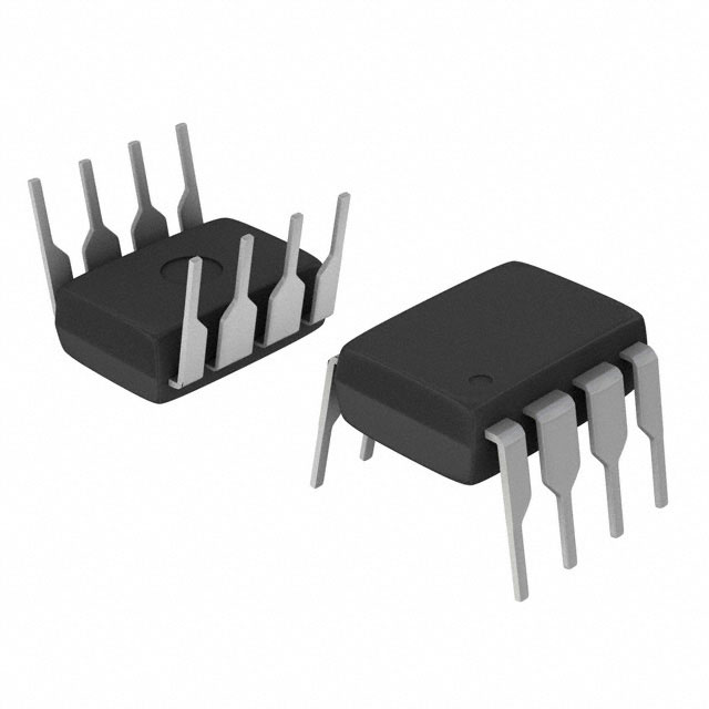
  • Package: The LMC6482AIN/NOPB is available in an 8-pin DIP tube package, facilitating easy integration into existing designs.
  • REACH and RoHS Compliance: The LMC6482AIN/NOPB is REACH unaffected and RoHS3 compliant, adhering to environmental regulations.

LMC6482AIN/NOPB Applications

The LMC6482AIN/NOPB is well-suited for a variety of applications due to its high performance and low power consumption. Ideal use cases include:

  • Audio Amplification: The low distortion and high slew rate make it perfect for audio signal processing.
  • Sensor Signal Conditioning: The low input bias current and low voltage offset are crucial for accurate sensor readings.
  • Industrial Control Systems: The wide supply voltage range and robust performance make it suitable for industrial applications.
  • Data Acquisition Systems: The LMC6482AIN/NOPB's high-speed performance is beneficial in data acquisition systems requiring fast signal processing.

Conclusion of LMC6482AIN/NOPB

The LMC6482AIN/NOPB from Texas Instruments stands out in the market due to its combination of high performance, low power consumption, and compliance with environmental regulations. Its wide supply voltage range, low input bias current, and high slew rate make it an excellent choice for applications requiring precision and speed. Whether used in audio amplification, sensor signal conditioning, or industrial control systems, the LMC6482AIN/NOPB delivers reliable and efficient performance.

Tech Specifications

Number of Channels per Chip
Unit Weight
Power Supply Type
Typical Output Current (mA)
Rail-to-rail
Product
PPAP
Gain Bandwidth Product
Automotive
Maximum Input Offset Current (uA)
RoHS
REACH Status
Input common mode headroom (to negative supply) (typ) (V)
Operating temperature range (°C)
PSRR - Power Supply Rejection Ratio
Current - Supply
Output swing headroom (to negative supply) (typ) (V)
Standard Package Name
Shut Down Support
Mounting
Minimum Single Supply Voltage (V)
Iout (typ) (A)
Manufacturer Type
Package
Minimum CMRR (dB)
Total supply voltage (+5 V = 5, ±5 V = 10) (max) (V)
GBW (typ) (MHz)
en - Input Voltage Noise Density
Output Type
Vos - Input Offset Voltage
Minimum CMRR Range (dB)
Process Technology
Typical Gain Bandwidth Product (MHz)
Package Height
Maximum Operating Temperature
Ib - Input Bias Current
Width
RoHS Status
Number of channels
Iq per channel (typ) (mA)
Minimum Operating Temperature
Voltage - Input Offset
Type
Vos (offset voltage at 25°C) (max) (mV)
Length
Operating Supply Voltage
Output Current per Channel
Part Status
Supply Type
Lead finish / Ball material
Number of Circuits
Package Width
GBP - Gain Bandwidth Product
Voltage - Supply Span (Max)
Maximum Input Offset Voltage (mV)
Product Status
Current - Input Bias
Rail to Rail
Supplier Package
Package / Case
Number of Channels
Typical Voltage Gain (dB)
Technology
Typical Input Bias Current (uA)
EU RoHS
Carrier
Amplifier Type
Maximum Dual Supply Voltage (V)
Input common mode headroom (to positive supply) (typ) (V)
Moisture Sensitivity Level (MSL)
Typical Input Noise Voltage Density (nV/rtHz)
Operating Temperature
Architecture
Typical Slew Rate (V/us)
Output swing headroom (to positive supply) (typ) (V)
ECCN
MSL rating / Peak reflow
Mounting Type
THD + N at 1 kHz (typ) (%)
Pin Count
In - Input Noise Current Density
Minimum PSRR (dB)
Shutdown
Typical Dual Supply Voltage (V)
Voltage - Supply Span (Min)
Lead Shape
HTSUS
Pins
Current - Output / Channel
USHTS
PCB changed
HTS
Voltage Gain dB
Rating
ECCN (US)
Total supply voltage (+5 V = 5, ±5 V = 10) (min) (V)
Supplier Device Package
Supply Voltage - Min
Minimum Operating Temperature (°C)
Maximum Operating Temperature (°C)
Operating Supply Current
SR - Slew Rate
Mfr
Height
CMRR (typ) (dB)
Supply Voltage - Max
Offset drift (typ) (µV/°C)
Mounting Style
Input Type
Maximum Input Bias Current (uA)
Typical Noninverting Input Current Noise Density (pA/rtHz)
Slew Rate
Package Length
Minimum Dual Supply Voltage (V)
Vn at 1 kHz (typ) (nV√Hz)
Maximum Supply Current (mA)
CMRR - Common Mode Rejection Ratio
REACH
Series
Maximum Single Supply Voltage (V)
Slew rate (typ) (V/µs)
Base Product Number

LMC6482AIN/NOPB Documents

Download datasheets and manufacturer documentation for LMC6482AIN/NOPB

Ersa Mechanical Outline Drawing      
Ersa Process change notification (PDF)       Qualification of New Mold Compound for selected Devices in the PDIP package (PDF)       Product Change Notification (PDF)       Product Change Notification 2024-04-12 (PDF)       Product Change Notification 2024-04-02 (PDF)      
Ersa LMC6482AIN/NOPB Symbol & Footprint by SnapMagic      
Ersa LMC6482 TINA-TI Reference Design       LMC6482 TINA-TI Reference Design (Rev. A)      
Ersa LMC6482 TINA-TI Spice Model       LMC6482 PSPICE Model (Rev. A)       LMC6482 PSPICE Model (Rev. B)       LMC6482 TINA-TI Spice Model (Rev. A)      

Shopping Guide

Payment Methods
Payment Methods include Prepayment TT (bank transfer), Western Union, and PayPal. Customers are responsible for shipping costs, bank charges, customs duties and taxes.
Shipping Rate
Shipments are made once a day around 5pm, excluding Sundays. Once shipped, the estimated delivery time is usually 5-7 business days, depending on the courier you choose.
Delivery Methods
Provide DHL, FedEx, UPS, EMS, SF Express and Registered Airmail International Delivery Service