
Texas Instruments
THS4503ID
OP Amps, Buffer Amps ICs


.png?x-oss-process=image/format,webp/resize,p_30)


THS4503ID Description
THS4503ID Description
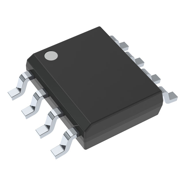
The THS4503ID from Texas Instruments is a high-performance, fully differential amplifier designed for precision signal conditioning in demanding applications. Packaged in an 8-SOIC tube, this ROHS3 Compliant and REACH Unaffected IC operates over a 4.5V to 15V supply range, delivering exceptional performance with a 300 MHz gain bandwidth product (GBW) and a 370 MHz -3dB bandwidth. Its differential output architecture ensures superior noise immunity, making it ideal for high-speed data acquisition, communications, and medical imaging systems. With a slew rate of 2800V/µs and 120 mA output current capability, the THS4503ID excels in driving low-impedance loads while maintaining signal integrity.
THS4503ID Features
- High-Speed Performance: 300 MHz GBW and 370 MHz bandwidth enable precise signal amplification in RF and broadband applications.
- Low Input Bias Current: 4 µA minimizes errors in high-impedance sensor interfaces.
- Robust Output Drive: 120 mA/channel current output supports demanding loads like ADCs or transmission lines.
- Wide Supply Range: 4.5V to 15V operation accommodates diverse system requirements.
- Low Offset Voltage: 1 mV ensures accuracy in precision analog circuits.
- Surface-Mount Package: 8-SOIC (Tube) for compact PCB designs and automated assembly.
THS4503ID Applications
The THS4503ID is optimized for:
- High-Speed Data Converters: Acts as a differential driver for ADCs in test equipment or radar systems.
- Medical Imaging: Enhances signal fidelity in ultrasound and MRI front-end circuits.
- Communications Infrastructure: Supports RF signal conditioning in 5G base stations and optical transceivers.
- Industrial Instrumentation: Ideal for high-bandwidth sensor interfaces and control systems.
Conclusion of THS4503ID
The THS4503ID stands out as a versatile, high-speed differential amplifier, combining wide bandwidth, high slew rate, and robust output drive in a compact package. Its low noise, precision performance, and broad supply range make it a top choice for engineers designing advanced analog systems. Whether in medical, communications, or industrial applications, the THS4503ID delivers reliability and performance unmatched by conventional op-amps.
Tech Specifications
THS4503ID Documents
Download datasheets and manufacturer documentation for THS4503ID
 THS4502/03
  THS4502/03
 Shopping Guide


.png?x-oss-process=image/format,webp/resize,h_32)


