

Texas Instruments
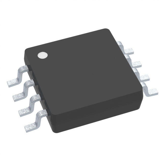
LMV358IDGKRG4
OP Amps, Buffer Amps ICs

Not available to buy online? Want the lower wholesale price? Please Send RFQ to get best price, we will respond immediately


.png?x-oss-process=image/format,webp/resize,p_30)


LMV358IDGKRG4 Description
LMV358IDGKRG4 Description
The LMV358IDGKRG4 is a general-purpose operational amplifier (op amp) from Texas Instruments, designed for a wide range of applications requiring high performance and reliability. This dual-channel op amp is housed in an 8-pin VSSOP package, making it suitable for surface-mount applications. It features a supply voltage range of 2.7 V to 5.5 V, allowing it to operate efficiently in both low-power and standard voltage systems.
LMV358IDGKRG4 Features
- Wide Supply Voltage Range: The LMV358IDGKRG4 operates within a supply voltage span of 2.7 V to 5.5 V, providing flexibility for various power supply configurations.
- High Gain Bandwidth Product: With a gain bandwidth product of 1 MHz, this op amp delivers high-frequency performance suitable for signal processing and filtering applications.
- Low Input Bias Current: The low input bias current of 15 nA ensures minimal loading on the input signal source, making it ideal for high-impedance applications.
- Low Supply Current: The device consumes only 210 µA per channel, making it energy-efficient and suitable for battery-powered and low-power applications.
- High Slew Rate: A slew rate of 1 V/µs allows the op amp to handle fast-changing signals without significant distortion.
- Low Input Offset Voltage: The low input offset voltage of 1.7 mV ensures high accuracy in signal amplification and processing.
- High Output Current: Each channel can deliver up to 40 mA of output current, enabling the op amp to drive a wide range of loads.
- Compliance and Packaging: The LMV358IDGKRG4 is ROHS3 compliant and REACH unaffected, ensuring environmental and regulatory compliance. It is packaged in a tape and reel (TR) format, facilitating automated assembly processes.
LMV358IDGKRG4 Applications
The LMV358IDGKRG4 is ideal for a variety of applications due to its versatile performance characteristics. Some specific use cases include:
- Signal Conditioning: The low input bias current and low input offset voltage make it suitable for precision signal conditioning in sensors and transducers.
- Audio Amplification: The high slew rate and wide supply voltage range enable high-fidelity audio amplification in consumer electronics.
- Analog Filters: The high gain bandwidth product and low supply current make it ideal for designing active filters in signal processing circuits.
- Battery-Powered Devices: The low power consumption and wide operating voltage range make it suitable for portable and battery-powered applications.
- Industrial Control Systems: The robust performance and compliance with environmental regulations make it a reliable choice for industrial control and automation systems.
Conclusion of LMV358IDGKRG4
The LMV358IDGKRG4 from Texas Instruments is a versatile and high-performance dual-channel operational amplifier that offers a balance of power efficiency, accuracy, and bandwidth. Its wide supply voltage range, low input bias current, and high slew rate make it suitable for a variety of applications, from precision signal conditioning to audio amplification. The device's compliance with environmental regulations and its surface-mount packaging further enhance its appeal for modern electronics design. Whether in consumer electronics, industrial systems, or portable devices, the LMV358IDGKRG4 provides reliable performance and exceptional value.
Tech Specifications
LMV358IDGKRG4 Documents
Download datasheets and manufacturer documentation for LMV358IDGKRG4
Mechanical Outline Drawing Product Change Notification (PDF) LMV358IDGKRG4 Symbol & Footprint by SnapMagic Inverting Amplifier Circuit (Rev. C) Related Parts


Shopping Guide


.png?x-oss-process=image/format,webp/resize,h_32)


©2025 ERSA Electronics Corporation.