
Texas Instruments
LMV842QMA/NOPB
OP Amps, Buffer Amps ICs


.png?x-oss-process=image/format,webp/resize,p_30)


LMV842QMA/NOPB Description
LMV842QMA/NOPB Description
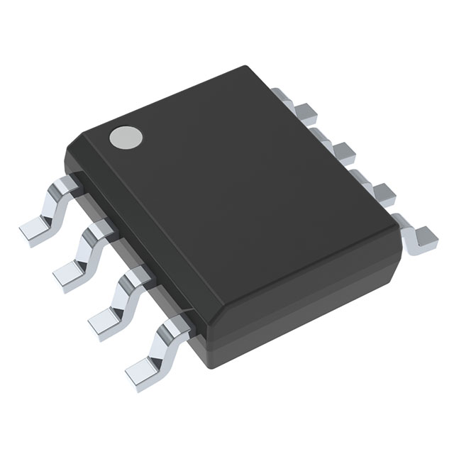
The LMV842QMA/NOPB is a high-performance, general-purpose operational amplifier from Texas Instruments, designed for demanding automotive applications. This dual-channel op-amp offers a wide supply voltage range from 2.7 V to 12 V, making it suitable for various power supply configurations. It features a gain bandwidth product of 4.5 MHz, ensuring high-frequency performance and stability. The LMV842QMA/NOPB also boasts an impressively low input bias current of 0.3 pA and an input offset voltage of 50 µV, which contribute to its precision and reliability.
LMV842QMA/NOPB Features
- Wide Supply Voltage Range: Operates from 2.7 V to 12 V, providing flexibility in power supply design.
- High Gain Bandwidth Product: 4.5 MHz ensures robust performance in high-frequency applications.
- Low Input Bias Current: 0.3 pA minimizes the impact of input currents on signal integrity.
- Low Input Offset Voltage: 50 µV ensures high accuracy and precision in signal processing.
- High Slew Rate: 2.5 V/µs allows for fast response times and accurate signal reproduction.
- Automotive Grade: Certified for use in automotive applications, ensuring reliability and robustness.
- Compliance: ROHS3 compliant and REACH unaffected, meeting environmental and regulatory standards.
- Moisture Sensitivity Level: MSL 1 (Unlimited) ensures the device is safe from moisture damage during storage and handling.
- Package Type: Supplied in a tube package, suitable for surface mount applications.
LMV842QMA/NOPB Applications
The LMV842QMA/NOPB is ideal for a variety of applications, particularly in the automotive sector, where reliability and precision are paramount. Its wide supply voltage range and high performance make it suitable for:
- Automotive Electronics: Powertrain control units, infotainment systems, and advanced driver-assistance systems (ADAS).
- Signal Conditioning: Amplifying and conditioning signals in sensors and transducers.
- Analog-to-Digital Conversion: Driving ADCs with high precision and low noise.
- Power Management: Voltage regulation and monitoring in power supply circuits.
- Industrial Control Systems: Precision control and monitoring in industrial automation and process control.
Conclusion of LMV842QMA/NOPB
The LMV842QMA/NOPB from Texas Instruments is a versatile and high-performance operational amplifier tailored for automotive and industrial applications. Its wide supply voltage range, high gain bandwidth product, and low input bias current make it a reliable choice for precision signal processing. The device's automotive grade certification ensures robustness and reliability in demanding environments. With its compliance to ROHS3 and REACH standards, the LMV842QMA/NOPB meets the stringent environmental and regulatory requirements of modern electronics. Whether used in automotive electronics, signal conditioning, or power management, the LMV842QMA/NOPB delivers outstanding performance and reliability, making it a preferred choice for engineers and designers in the electronics industry.
Tech Specifications
LMV842QMA/NOPB Documents
Download datasheets and manufacturer documentation for LMV842QMA/NOPB
 LMV841-42, LMV844 Datasheet
  LMV841-42, LMV844 Datasheet
 Shopping Guide


.png?x-oss-process=image/format,webp/resize,h_32)


