
 German
 Japanese
 Portuguese
 Korea
Korea
 Mexico
 Dutch
Dutch


Texas Instruments
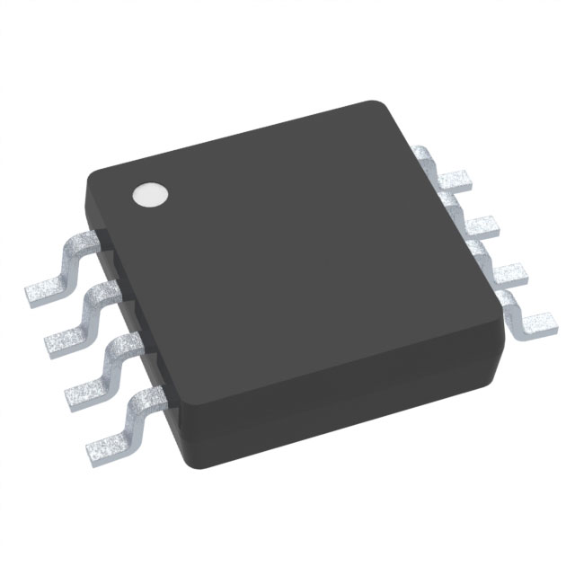
LMV932IDGKR

Why Choose Us?
Professional Platform
B2B & B2C purchasingDelivery at full speed
1-2 days deliveryWide variety
Original manufacturers365 days guarantee
Responsible quality
.png)


Tech Specifications
LMV932IDGKR Description
LMV932IDGKR Description
The LMV932IDGKR is a general-purpose operational amplifier (op-amp) from Texas Instruments, designed for a wide range of applications requiring high performance and reliability. This dual-channel op-amp is housed in an 8-pin VSSOP package, making it suitable for surface-mount applications. It operates within a supply voltage range of 1.8 V to 5 V, providing flexibility for various power supply configurations. The LMV932IDGKR features a gain bandwidth product of 1.5 MHz, a slew rate of 0.42 V/µs, and a low input bias current of 15 nA, ensuring high precision and stability in signal processing.
LMV932IDGKR Features
- Wide Supply Voltage Range: The LMV932IDGKR operates from 1.8 V to 5 V, making it suitable for both low-power and standard voltage applications.
- High Gain Bandwidth Product: With a gain bandwidth product of 1.5 MHz, this op-amp can handle high-frequency signals with minimal distortion.
- Low Input Bias Current: The low input bias current of 15 nA ensures high precision in signal amplification, making it ideal for sensitive applications.
- Dual-Channel Design: The dual-channel configuration allows for multiple signal processing paths, enhancing the versatility of the device.
- Low Supply Current: The device consumes only 116 µA per channel, making it energy-efficient and suitable for battery-powered applications.
- High Output Current: Each channel can deliver up to 100 mA, providing robust performance for driving various loads.
- Low Input Offset Voltage: The 1 mV input offset voltage ensures accurate signal processing and minimal error in the output signal.
- Surface-Mount Compatibility: The 8-pin VSSOP package is ideal for surface-mount applications, facilitating compact and reliable designs.
- Regulatory Compliance: The LMV932IDGKR is REACH unaffected and RoHS3 compliant, ensuring it meets environmental and safety standards.
LMV932IDGKR Applications
The LMV932IDGKR is well-suited for a variety of applications due to its versatile design and high performance. Some specific use cases include:
- Analog Signal Processing: Ideal for amplifying and conditioning analog signals in sensors, transducers, and other signal processing circuits.
- Audio Applications: Suitable for audio amplifiers, preamplifiers, and other audio processing circuits due to its high gain bandwidth and low distortion.
- Power Management: The low supply current and high output current make it suitable for power management circuits, including voltage regulators and power amplifiers.
- Industrial Control Systems: The wide supply voltage range and robust performance make it suitable for industrial control systems and automation applications.
- Consumer Electronics: Ideal for consumer electronics where compact size, low power consumption, and high performance are critical.
Conclusion of LMV932IDGKR
The LMV932IDGKR from Texas Instruments is a versatile and high-performance general-purpose op-amp that offers a wide range of features and benefits. Its wide supply voltage range, high gain bandwidth product, and low input bias current make it suitable for a variety of applications, from analog signal processing to power management. The dual-channel design and surface-mount compatibility further enhance its versatility and ease of integration. While the product is marked as obsolete, it remains a reliable choice for applications requiring high precision and reliability. For those seeking a robust and efficient op-amp solution, the LMV932IDGKR is an excellent option.
FAQ
Not available to buy online? Want the lower wholesale price? Please Send RFQ to get best price, we will respond immediately


.png?x-oss-process=image/format,webp/resize,h_32)


