
Texas Instruments
TLC277CDR
OP Amps, Buffer Amps ICs


.png?x-oss-process=image/format,webp/resize,p_30)


TLC277CDR Description
TLC277CDR Description
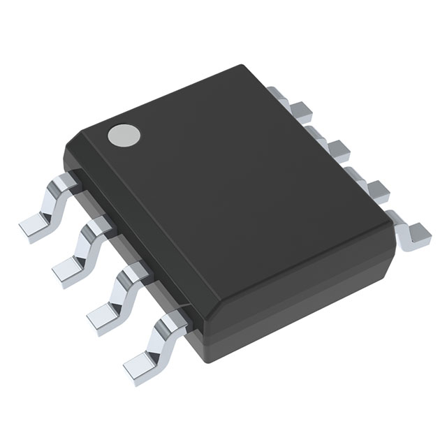
The TLC277CDR is a high-performance, dual-channel operational amplifier (op-amp) from Texas Instruments, designed for a wide range of applications in the electronics industry. This IC is part of the LinCMOS™ series, which is known for its low power consumption and high precision. The device operates within a supply voltage range of 3V to 16V, making it suitable for both low-voltage and standard voltage applications. It is compliant with RoHS3 and REACH standards, ensuring environmental responsibility in manufacturing.
TLC277CDR Features
- Voltage Supply Span: The TLC277CDR can operate with a supply voltage ranging from a minimum of 3V to a maximum of 16V, providing flexibility in power supply design.
- Gain Bandwidth Product: With a gain bandwidth product of 2.2 MHz, it offers high-speed performance for demanding applications.
- Slew Rate: The device boasts a fast slew rate of 5.3V/µs, which is crucial for applications requiring quick response times.
- Low Input Bias Current: The input bias current is an ultra-low 0.7 pA, which is beneficial for high-impedance input sources to maintain signal integrity.
- Low Voltage Input Offset: At 1.1 mV, the low input offset voltage ensures high accuracy in amplification.
- Supply Current: The TLC277CDR consumes only 1.9mA for both channels, making it energy-efficient.
- Output Current: Each channel can provide up to 30 mA of output current, suitable for driving various loads.
- Operating Temperature: The device is rated for operation between 0°C and 70°C, accommodating a wide range of environmental conditions.
- Mounting Type: Surface mount packaging allows for compact and efficient PCB layouts.
TLC277CDR Applications
The TLC277CDR is ideal for applications where precision, speed, and low power consumption are critical. Some specific use cases include:
- Audio Amplification: The low noise and high slew rate make it suitable for audio signal processing.
- Sensor Signal Conditioning: Its low input bias current and low offset voltage are beneficial for accurate sensor signal amplification.
- Data Acquisition Systems: The high-speed performance is ideal for fast data acquisition in industrial and scientific applications.
- Medical Equipment: The precision and reliability of the TLC277CDR make it suitable for use in medical devices requiring accurate signal amplification.
Conclusion of TLC277CDR
The TLC277CDR from Texas Instruments stands out for its combination of high-speed performance, low power consumption, and precision. Its dual-channel configuration and wide supply voltage range make it a versatile choice for a variety of applications in the electronics industry. The device's compliance with environmental standards and its robust performance specifications position it as a reliable component for demanding applications.
Tech Specifications
TLC277CDR Documents
Download datasheets and manufacturer documentation for TLC277CDR
 TLC272/A/B/Y, TLC277
  Mult Devices Font 21/Apr/2018 Mult Dev 30/Mar/2023
 Shopping Guide


.png?x-oss-process=image/format,webp/resize,h_32)


