
Texas Instruments
LT1054IDWG4
DC Switching Voltage Regulators


.png?x-oss-process=image/format,webp/resize,p_30)


LT1054IDWG4 Description
LT1054IDWG4 Description
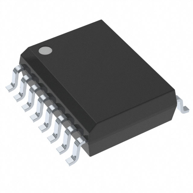
The LT1054IDWG4 is a high-performance charge pump voltage inverter designed by Texas Instruments, a leading manufacturer in the electronics industry. This integrated circuit (IC) is part of the Power Management (PMIC) category and is housed in a Tube package. The LT1054IDWG4 is specifically designed to provide an adjustable or fixed output voltage, making it versatile for a wide range of applications.
LT1054IDWG4 Features
- Output Type: The LT1054IDWG4 offers an adjustable or fixed output type, providing flexibility in voltage regulation.
- Input Voltage Range: It operates within a wide input voltage range of 3.5V to 15V, making it suitable for various power supply scenarios.
- Output Current: The IC can deliver a maximum output current of 100mA, ensuring reliable performance in applications requiring moderate current levels.
- Output Configuration: The LT1054IDWG4 supports both positive and negative output configurations, enhancing its versatility.
- Switching Frequency: With a switching frequency of 25kHz, it ensures efficient power conversion while minimizing noise and interference.
- Compliance and Standards: The LT1054IDWG4 is REACH unaffected and ROHS3 compliant, adhering to stringent environmental and safety regulations. It also has a moisture sensitivity level (MSL) of 1, indicating unlimited storage conditions.
- Topology: Utilizing a charge pump topology, the LT1054IDWG4 offers high efficiency and compact design.
- Mounting Type: The surface mount design facilitates easy integration into modern electronic systems.
- Output Voltage: The maximum output voltage is 26.4V, providing a wide range of voltage levels for different applications.
- Number of Outputs: It features a single output, simplifying the design and reducing complexity.
- Package: The Tube package ensures reliable handling and storage.
LT1054IDWG4 Applications
The LT1054IDWG4 is ideal for applications requiring an efficient and reliable voltage inverter. Its adjustable output and wide input voltage range make it suitable for:
- Power Supply Design: Ideal for creating compact and efficient power supply units.
- Battery-Powered Devices: Provides stable voltage inversion for devices powered by batteries.
- Industrial Equipment: Suitable for industrial applications where reliable power conversion is crucial.
- Consumer Electronics: Enhances the performance of consumer electronics by providing stable and efficient power regulation.
Conclusion of LT1054IDWG4
The LT1054IDWG4 from Texas Instruments is a robust and versatile charge pump voltage inverter that offers significant advantages over similar models. Its wide input voltage range, adjustable output, and high efficiency make it an excellent choice for a variety of applications. The LT1054IDWG4's compliance with environmental and safety standards further enhances its appeal for modern electronic designs. Whether used in power supply units, battery-powered devices, industrial equipment, or consumer electronics, the LT1054IDWG4 delivers reliable performance and efficient power conversion.
Tech Specifications
LT1054IDWG4 Documents
Download datasheets and manufacturer documentation for LT1054IDWG4
 Mechanical Outline Drawing
  Product Change Notification (PDF)
  LT1054IDWG4 Symbol & Footprint by SnapMagic
 Shopping Guide


.png?x-oss-process=image/format,webp/resize,h_32)


