
 German
 Japanese
 Portuguese
 Korea
Korea
 Mexico
 Dutch
Dutch


Texas Instruments
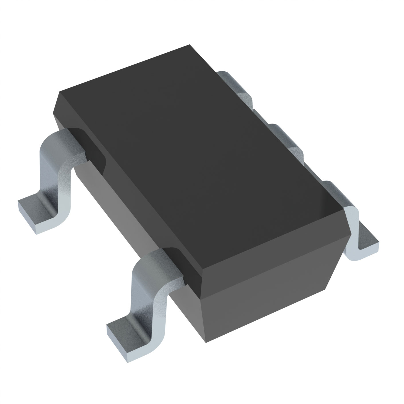
SN74AUP1G126DBVR

Why Choose Us?
Professional Platform
B2B & B2C purchasingDelivery at full speed
1-2 days deliveryWide variety
Original manufacturers365 days guarantee
Responsible quality
.png)


Tech Specifications
SN74AUP1G126DBVR Description
SN74AUP1G126DBVR Description
The SN74AUP1G126DBVR is a high-performance buffer from Texas Instruments, designed to provide reliable signal transmission in various electronic systems. This device is part of the 74AUP series, known for its robust performance and versatility. With a single bit per element and a single element configuration, it offers a compact solution for buffering applications. The device is surface mount, which allows for efficient use of space on printed circuit boards (PCBs), and it operates over a wide voltage supply range of 0.8V to 3.6V, making it suitable for low-power designs.
SN74AUP1G126DBVR Features
-
Technical Specifications: The SN74AUP1G126DBVR boasts a low supply voltage range, which is ideal for power-sensitive applications. It features an output high and low current of 4mA, ensuring consistent signal strength. The device is also designed to be moisture insensitive, with an MSL of 1, which means it can be stored and used in a wide range of environments without concern for moisture-related degradation.
-
Performance Benefits: This buffer is REACH unaffected and RoHS3 compliant, indicating its commitment to environmental standards. The device's wide operating voltage range and low power consumption make it an excellent choice for portable and battery-operated devices.
-
Unique Features and Advantages: The SN74AUP1G126DBVR stands out with its ability to operate over a broad voltage range, which is beneficial for systems that require flexibility in power supply. Its surface mount design also contributes to its compactness and ease of integration into dense PCB layouts.
SN74AUP1G126DBVR Applications
-
Ideal Use Cases: The SN74AUP1G126DBVR is ideal for applications where signal integrity and low power consumption are critical, such as in mobile devices, wearable technology, and IoT sensors. Its wide voltage range also makes it suitable for automotive electronics where power supply can vary.
-
Specific Applications: This buffer can be used in digital logic circuits to isolate or buffer signals, ensuring signal integrity over long traces or between different voltage domains. It is also useful in systems where space is at a premium, such as in consumer electronics and industrial control systems.
Conclusion of SN74AUP1G126DBVR
The SN74AUP1G126DBVR is a versatile and reliable buffer that offers a combination of low power consumption, wide voltage operation, and environmental compliance. Its unique features make it an excellent choice for a variety of applications where signal integrity and power efficiency are paramount. Texas Instruments' commitment to quality and performance ensures that this device will meet the demands of even the most challenging electronic designs.
FAQ
| Quantity | Unit Price | Ext. Price |
|---|---|---|
| 5+ | $0.15224 | $0.76 |
| 50+ | $0.14844 | $7.42 |
| 150+ | $0.14591 | $21.89 |
Not available to buy online? Want the lower wholesale price? Please Send RFQ to get best price, we will respond immediately


.png?x-oss-process=image/format,webp/resize,h_32)


