
 German
 Japanese
 Portuguese
 Korea
Korea
 Mexico
 Dutch
Dutch


Texas Instruments
CD4050BDR

Why Choose Us?
Professional Platform
B2B & B2C purchasingDelivery at full speed
1-2 days deliveryWide variety
Original manufacturers365 days guarantee
Responsible quality
.png)


Tech Specifications
CD4050BDR Description
CD4050BDR Description
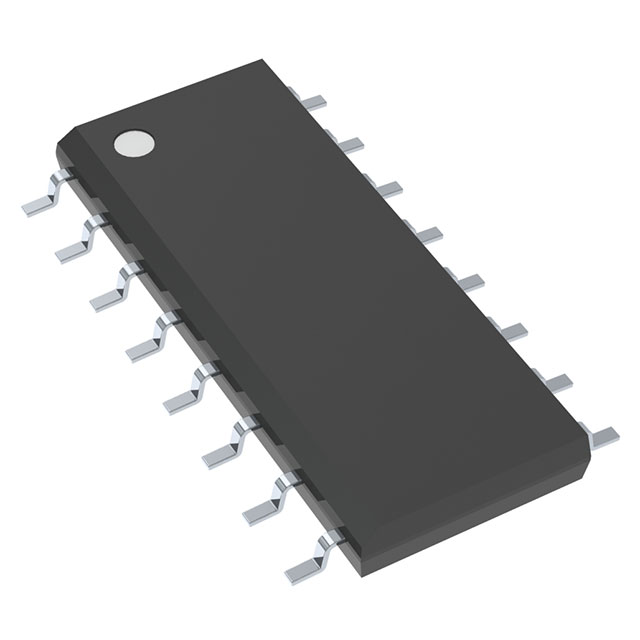
The CD4050BDR is a high-performance buffer, manufactured by Texas Instruments, designed for applications requiring non-inverting signal transmission. With a supply voltage range of 3V to 18V, this device is versatile and can be used in a wide range of electronic systems. The CD4050BDR is part of the 4000B series and is currently active, ensuring ongoing availability and support. It is packaged in a 16-SOIC package, suitable for surface mount applications, and is available in tape and reel packaging for efficient handling and integration into automated assembly processes.
CD4050BDR Features
-
Technical Specifications: The CD4050BDR operates on a single bit per element, making it ideal for simple signal buffering applications. It boasts a low output high current of 8mA and a high output low current of 48mA, ensuring reliable signal transmission even under varying load conditions. The device is RoHS3 compliant, indicating its adherence to environmental regulations, and is unaffected by REACH, further ensuring its suitability for a wide range of applications.
-
Performance Benefits: The CD4050BDR's wide supply voltage range and high output currents make it a robust choice for buffering applications. Its surface mount design allows for compact integration into densely populated circuit boards, while the unlimited moisture sensitivity level (MSL 1) ensures reliable performance in various environmental conditions.
-
Unique Features and Advantages: Compared to similar models, the CD4050BDR stands out with its wide supply voltage range, which makes it suitable for a broader range of applications. Its high output currents also provide an advantage in high-load scenarios, ensuring signal integrity.
CD4050BDR Applications
The CD4050BDR is ideal for a variety of applications where signal buffering is required without signal inversion. Some specific use cases include:
-
Digital Signal Processing: In digital systems where signal integrity is crucial, the CD4050BDR can be used to buffer signals to ensure they are transmitted accurately without degradation.
-
Automotive Electronics: The device's wide voltage range and robust performance make it suitable for automotive applications where reliability and durability are paramount.
-
Industrial Control Systems: In industrial settings, the CD4050BDR can be used to buffer signals in control systems, ensuring that commands are transmitted accurately and reliably.
Conclusion of CD4050BDR
The CD4050BDR is a versatile and reliable buffer from Texas Instruments, designed to meet the demands of modern electronic systems. Its wide supply voltage range, high output currents, and RoHS3 compliance make it an excellent choice for a variety of applications, from digital signal processing to automotive electronics. With its unique features and advantages over similar models, the CD4050BDR is a robust solution for buffering applications where signal integrity and reliability are critical.
FAQ
| Quantity | Unit Price | Ext. Price |
|---|---|---|
| 10+ | $0.46972 | $4.70 |
| 30+ | $0.42172 | $12.65 |
| 100+ | $0.36000 | $36.00 |
| 500+ | $0.33257 | $166.28 |
| 1000+ | $0.28628 | $286.28 |
Not available to buy online? Want the lower wholesale price? Please Send RFQ to get best price, we will respond immediately


.png?x-oss-process=image/format,webp/resize,h_32)


