
Texas Instruments
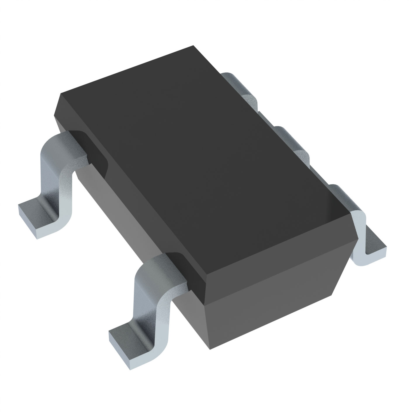
SN74AUP1G17DBVR
Buffers, Drivers, Receivers, Transceivers


- 5+
- $0.12046
- $0.6
- 50+
- $0.09625
- $4.81
- 150+
- $0.08414
- $12.62
- 500+
- $0.07507
- $37.53

.png?x-oss-process=image/format,webp/resize,p_30)


SN74AUP1G17DBVR Description
SN74AUP1G17DBVR Description
The SN74AUP1G17DBVR is a high-performance buffer from Texas Instruments, designed to meet the demands of modern electronic systems. This device features a Schmitt Trigger input, ensuring reliable signal detection and noise immunity. With a single-bit per element and a voltage supply range of 0.8V to 3.6V, it is suitable for low-voltage applications. The SN74AUP1G17DBVR is RoHS3 compliant, REACH unaffected, and EAR99 classified, making it compliant with international regulations.
SN74AUP1G17DBVR Features
- Input Type: Schmitt Trigger for improved signal detection and noise immunity.
- Voltage - Supply: 0.8V to 3.6V, suitable for low-voltage applications.
- Number of Bits per Element: 1, providing efficient signal buffering.
- Mounting Type: Surface Mount, ideal for compact and space-constrained designs.
- Series: 74AUP, known for its high-speed performance and low power consumption.
- Current - Output High, Low: 4mA, ensuring consistent output performance.
- Moisture Sensitivity Level (MSL): 1 (Unlimited), suitable for a wide range of environmental conditions.
SN74AUP1G17DBVR Applications
The SN74AUP1G17DBVR is ideal for various applications where high-speed signal buffering is required. Some specific use cases include:
- Communication Systems: For buffering signals in high-speed data transmission lines.
- Automotive Electronics: In infotainment systems and sensor interfaces where reliable signal transmission is crucial.
- Industrial Control Systems: For buffering signals in PLCs and motor control applications.
- Consumer Electronics: In portable devices and home automation systems where low power consumption and high-speed signal processing are essential.
Conclusion of SN74AUP1G17DBVR
The SN74AUP1G17DBVR from Texas Instruments is a versatile and high-performance buffer, offering unique features such as Schmitt Trigger input and a wide voltage supply range. Its compliance with international regulations and suitability for various applications make it an excellent choice for designers looking to enhance the performance and reliability of their electronic systems. With its robust specifications and proven performance, the SN74AUP1G17DBVR is a reliable component for high-speed signal buffering in a wide range of applications.
Tech Specifications
SN74AUP1G17DBVR Documents
Download datasheets and manufacturer documentation for SN74AUP1G17DBVR
 Assembly Site 15/Nov/2023
  SN74AUP1G17 Datasheet
  SN74AUP1G17 Datasheet
  SN74AUP1G17 18/Oct/2017 Die Conversion Revision A 19/Feb/2015
 Shopping Guide


.png?x-oss-process=image/format,webp/resize,h_32)


