
 German
 Japanese
 Portuguese
 Korea
Korea
 Mexico
 Dutch
Dutch


Texas Instruments
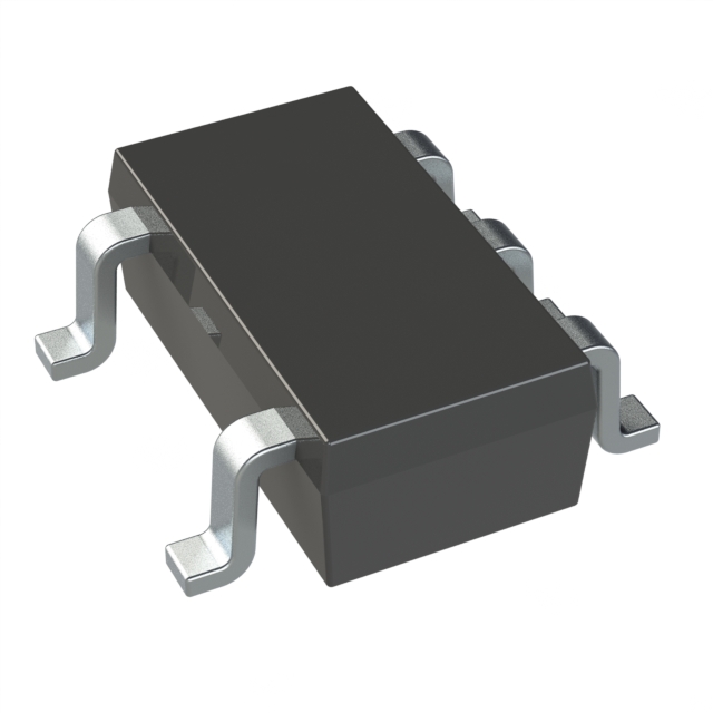
OPA207IDBVR

Why Choose Us?
Professional Platform
B2B & B2C purchasingDelivery at full speed
1-2 days deliveryWide variety
Original manufacturers365 days guarantee
Responsible quality
.png)


Tech Specifications
OPA207IDBVR Description
The OPA207IDBVR is a high-performance operational amplifier (op-amp) from Texas Instruments. It is designed for use in a wide range of applications, including audio, video, and precision instrumentation circuits.
Description:
The OPA207IDBVR is a monolithic operational amplifier that combines high speed, low distortion, and low noise characteristics. It is available in a small 8-pin VSSOP package, making it ideal for use in portable and battery-powered applications.
Features:
- High speed: The OPA207IDBVR has a high slew rate of 20 V/µs, making it suitable for use in high-speed applications.
- Low distortion: The op-amp has a low total harmonic distortion (THD) of -93 dB, which is ideal for use in audio applications.
- Low noise: The OPA207IDBVR has a low input voltage noise of 5.2 nV/√Hz, which makes it suitable for use in precision instrumentation circuits.
- Wide supply voltage range: The op-amp can operate from a supply voltage range of 3V to 36V, making it suitable for use in a wide range of applications.
- Low input bias current: The OPA207IDBVR has a low input bias current of 1 pA, which reduces input offset errors in precision circuits.
Applications:
The OPA207IDBVR is suitable for use in a wide range of applications, including:
- Audio circuits: The low distortion and low noise characteristics of the OPA207IDBVR make it ideal for use in audio circuits, such as preamplifiers and headphone amplifiers.
- Video circuits: The high speed and low distortion characteristics of the op-amp make it suitable for use in video circuits, such as analog-to-digital converters.
- Precision instrumentation circuits: The low noise and low input bias current characteristics of the OPA207IDBVR make it suitable for use in precision instrumentation circuits, such as strain gauge amplifiers and pressure sensors.
- Battery-powered applications: The wide supply voltage range and low power consumption of the OPA207IDBVR make it ideal for use in battery-powered applications, such as portable audio equipment and medical devices.
In summary, the OPA207IDBVR is a high-performance operational amplifier that offers high speed, low distortion, and low noise characteristics. It is suitable for use in a wide range of applications, including audio, video, and precision instrumentation circuits, as well as battery-powered applications.
FAQ
| Quantity | Unit Price | Ext. Price |
|---|---|---|
| 1+ | $2.22515 | $2.23 |
| 10+ | $2.17028 | $21.70 |
| 30+ | $2.13428 | $64.03 |
Not available to buy online? Want the lower wholesale price? Please Send RFQ to get best price, we will respond immediately


.png?x-oss-process=image/format,webp/resize,h_32)


