Texas Instruments_OPA2156IDGKR

Texas Instruments
OPA2156IDGKR  
OP Amps, Buffer Amps ICs

Texas Instruments
OPA2156IDGKR
687-OPA2156IDGKR
Ersa
Texas Instruments-OPA2156IDGKR-datasheets-3829072.pdf
IC CMOS 2 CIRCUIT 8VSSOP
In Stock : 6363

Not available to buy online? Want the lower wholesale price? Please Send RFQ to get best price, we will respond immediately

QUICK RFQ
ADD TO RFQ LIST
ersa FreeSample ersa flow
ISO9001
Quality Policy
ISO45001
ISO14001

OPA2156IDGKR Description

The OPA2156IDGKR is a precision operational amplifier (op-amp) from Texas Instruments. It is designed for high-speed, low-distortion applications and offers excellent precision and performance.

Description:

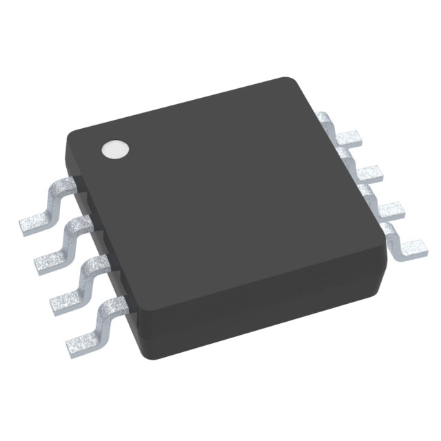
The OPA2156IDGKR is a dual operational amplifier that features a high slew rate of 4.5 V/µs and a low input bias current of 1 pA. It operates over a wide supply voltage range of ±2.5V to ±18V and has a low input offset voltage drift of 1 µV/°C. The device is available in a small 8-pin SOIC package.

Features:

  • Dual operational amplifier
  • High slew rate: 4.5 V/µs
  • Low input bias current: 1 pA
  • Wide supply voltage range: ±2.5V to ±18V
  • Low input offset voltage drift: 1 µV/°C
  • Precision performance
  • Low distortion
  • Short-circuit protection

Applications:

The OPA2156IDGKR is suitable for a wide range of high-speed, precision applications, including:

  1. Audio processing
  2. Video processing
  3. Data acquisition systems
  4. Strain gauge amplifiers
  5. Medical instrumentation
  6. Test and measurement equipment
  7. Industrial control systems

In summary, the OPA2156IDGKR is a high-performance dual operational amplifier from Texas Instruments that offers excellent precision and performance for a wide range of applications. Its high slew rate, low input bias current, and low input offset voltage drift make it ideal for high-speed, low-distortion applications.

Tech Specifications

Number of Channels per Chip
Unit Weight
Power Supply Type
Typical Output Current (mA)
Rail-to-rail
PPAP
Gain Bandwidth Product
Automotive
Maximum Input Offset Current (uA)
RoHS
REACH Status
Input common mode headroom (to negative supply) (typ) (V)
Operating temperature range (°C)
Supplier Temperature Grade
Current - Supply
Output swing headroom (to negative supply) (typ) (V)
Standard Package Name
Shut Down Support
Mounting
Minimum Single Supply Voltage (V)
Iout (typ) (A)
Moisture Sensitive
Manufacturer Type
Package
Minimum CMRR (dB)
Maximum Quiescent Current (mA)
Total supply voltage (+5 V = 5, ±5 V = 10) (max) (V)
GBW (typ) (MHz)
en - Input Voltage Noise Density
Output Type
Vos - Input Offset Voltage
Minimum CMRR Range (dB)
Typical Gain Bandwidth Product (MHz)
Package Height
Maximum Operating Temperature
Ib - Input Bias Current
RoHS Status
Number of channels
Iq per channel (typ) (mA)
Minimum Operating Temperature
Voltage - Input Offset
Type
Vos (offset voltage at 25°C) (max) (mV)
Output Current per Channel
Part Status
Input Offset Voltage Drift (uV/°C)
Lead finish / Ball material
Number of Circuits
Package Width
GBP - Gain Bandwidth Product
Voltage - Supply Span (Max)
Maximum Input Offset Voltage (mV)
Typical Output Resistance (Ohm)
Product Status
Current - Input Bias
Rail to Rail
Supplier Package
Package / Case
Number of Channels
Typical Voltage Gain (dB)
Typical Input Bias Current (uA)
EU RoHS
Carrier
Amplifier Type
Maximum Dual Supply Voltage (V)
Input common mode headroom (to positive supply) (typ) (V)
Moisture Sensitivity Level (MSL)
Typical Input Noise Voltage Density (nV/rtHz)
Operating Temperature
Architecture
Typical Slew Rate (V/us)
Output swing headroom (to positive supply) (typ) (V)
ECCN
MSL rating / Peak reflow
Mounting Type
Pin Count
Minimum PSRR (dB)
Shutdown
Typical Dual Supply Voltage (V)
Voltage - Supply Span (Min)
Lead Shape
HTSUS
Pins
Current - Output / Channel
USHTS
PCB changed
HTS
Rating
ECCN (US)
Total supply voltage (+5 V = 5, ±5 V = 10) (min) (V)
Supplier Device Package
Supply Voltage - Min
Minimum Operating Temperature (°C)
Maximum Operating Temperature (°C)
Operating Supply Current
SR - Slew Rate
Mfr
CMRR (typ) (dB)
Supply Voltage - Max
Offset drift (typ) (µV/°C)
Mounting Style
Maximum Input Bias Current (uA)
Typical Noninverting Input Current Noise Density (pA/rtHz)
Slew Rate
Package Length
Minimum Dual Supply Voltage (V)
Vn at 1 kHz (typ) (nV√Hz)
CMRR - Common Mode Rejection Ratio
REACH
Series
Maximum Single Supply Voltage (V)
Slew rate (typ) (V/µs)
Typical Settling Time (ns)
Base Product Number
Input bias current (max) (pA)

OPA2156IDGKR Documents

Download datasheets and manufacturer documentation for OPA2156IDGKR

Ersa VSSOP Devices 12/May/2022      
Ersa OPA2156      
Ersa Marking change 01/Feb/2023      
Ersa 8-VSSOP      
Ersa OPA2156      

Shopping Guide

Payment Methods
Payment Methods include Prepayment TT (bank transfer), Western Union, and PayPal. Customers are responsible for shipping costs, bank charges, customs duties and taxes.
Shipping Rate
Shipments are made once a day around 5pm, excluding Sundays. Once shipped, the estimated delivery time is usually 5-7 business days, depending on the courier you choose.
Delivery Methods
Provide DHL, FedEx, UPS, EMS, SF Express and Registered Airmail International Delivery Service