
Texas Instruments
THS3091D
OP Amps, Buffer Amps ICs


.png?x-oss-process=image/format,webp/resize,p_30)


THS3091D Description
THS3091D Description
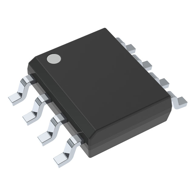
The THS3091D from Texas Instruments is a high-performance current feedback amplifier (CFA) designed for demanding applications requiring wide bandwidth and high slew rate. Packaged in an 8-SOIC tube, this single-channel op-amp operates over a 10V to 30V supply range, delivering 235 MHz bandwidth and an exceptional 7300V/µs slew rate. With a 280 mA output current capability and low 4 µA input bias current, it excels in driving low-impedance loads while maintaining signal integrity. The device is ROHS3 compliant and REACH unaffected, making it suitable for environmentally conscious designs.
THS3091D Features
- Current Feedback Architecture: Enables high-speed performance with minimal phase distortion.
- Wide Supply Range (10V–30V): Supports flexible power configurations.
- Ultra-High Slew Rate (7300V/µs): Ideal for fast transient response in pulse and video applications.
- High Output Current (280 mA): Drives heavy loads without external buffering.
- Low Input Bias Current (4 µA): Reduces errors in high-impedance circuits.
- 235 MHz Bandwidth: Ensures signal fidelity in high-frequency systems.
- MSL 1 (Unlimited): Suitable for extended storage and handling.
THS3091D Applications
The THS3091D is optimized for high-speed signal conditioning, including:
- Video Distribution Systems: Maintains signal integrity in HD/4K video lines.
- Test & Measurement Equipment: Delivers precise amplification for oscilloscopes and signal generators.
- RF/IF Signal Processing: Supports wideband amplification in communication systems.
- Pulse and Data Acquisition: High slew rate ensures accurate reproduction of fast edges.
- Active Filters and Buffers: Low distortion and high bandwidth enhance filter performance.
Conclusion of THS3091D
The THS3091D stands out for its blend of speed, power, and precision, making it a top choice for engineers designing high-performance analog systems. Its current feedback topology and robust output drive capability address challenges in video, RF, and instrumentation applications. While marked as Last Time Buy, its technical merits ensure it remains a viable solution for legacy and new designs requiring uncompromising performance.
Tech Specifications
THS3091D Documents
Download datasheets and manufacturer documentation for THS3091D
 THS3091, THS3095
  THS3091D(DR)/THS3095D obs 07/Mar/2023
  THS3091, THS3095
  THS309x Datasheet 22/May/2023 Design 25/Feb/2022
 Shopping Guide


.png?x-oss-process=image/format,webp/resize,h_32)


