
Texas Instruments
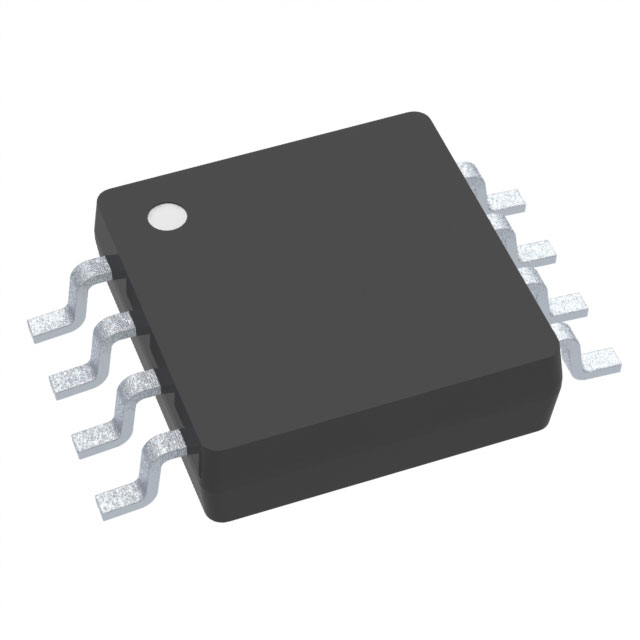
OPA2320AIDGKR
OP Amps, Buffer Amps ICs


- 1+
- $1.98886
- $1.99
- 10+
- $1.69906
- $16.99
- 30+
- $1.51855
- $45.56
- 100+
- $1.33474
- $133.47
- 500+
- $1.25028
- $625.14
- 1000+
- $1.21385
- $1213.85

.png?x-oss-process=image/format,webp/resize,p_30)


OPA2320AIDGKR Description
OPA2320AIDGKR Description
The OPA2320AIDGKR is a high-performance, dual operational amplifier from Texas Instruments, designed to deliver exceptional performance in various applications. This CMOS-based amplifier is known for its robustness and versatility, making it an ideal choice for a wide range of electronic systems. With a supply voltage range of 1.8V to 5.5V, it offers flexibility in power supply design. The OPA2320AIDGKR is compliant with RoHS3 standards and is unaffected by REACH regulations, ensuring environmental compliance.
OPA2320AIDGKR Features
- Voltage - Supply Span (Max): 5.5 V, providing flexibility in power supply design.
- Gain Bandwidth Product: 20 MHz, ensuring high-speed operation.
- Current - Input Bias: 0.2 pA, contributing to low power consumption and high precision.
- Slew Rate: 10V/µs, enabling rapid response times.
- Current - Supply: 1.45mA, ensuring efficient power usage.
- Voltage - Input Offset: 40 µV, contributing to high accuracy.
- Moisture Sensitivity Level (MSL): 2 (1 Year), indicating a robust design.
- Mounting Type: Surface Mount, suitable for modern PCB designs.
- Number of Circuits: 2, providing dual amplification in a single package.
- Current - Output / Channel: 65 mA, capable of driving various loads.
OPA2320AIDGKR Applications
The OPA2320AIDGKR is ideal for applications that require high-speed, low-noise amplification. Some specific use cases include:
- Audio Processing: Its low noise and high bandwidth make it suitable for audio signal amplification.
- Data Acquisition Systems: The high slew rate and low input bias current are beneficial for precise signal processing.
- Sensor Signal Conditioning: The dual channel configuration allows for simultaneous amplification of multiple sensor inputs.
- Industrial Control Systems: The robust design and wide supply voltage range make it suitable for harsh industrial environments.
Conclusion of OPA2320AIDGKR
The OPA2320AIDGKR stands out for its combination of high-speed performance, low power consumption, and dual channel capability. Its compliance with environmental standards and wide supply voltage range make it a versatile choice for a variety of applications in the electronics industry. Whether used in audio processing, data acquisition, or industrial control systems, the OPA2320AIDGKR delivers reliable and efficient amplification.
Tech Specifications
OPA2320AIDGKR Documents
Download datasheets and manufacturer documentation for OPA2320AIDGKR
 Mechanical Outline Drawing Function Diagram
  Add Cu as Alternate Wire Base Metal for Selected Device(s) on DGK and DGS packages (PDF) Product Change Notification (PDF)
  OPA2320AIDGKR Symbol & Footprint by SnapMagic
  Cascading Precision Op Amp Stages for Optimal AC and DC Performance OPA320 OPA320S OPA2320 OPA2320S EMI Immunity Performance
  OPAy320 Family TINA-TI Reference Design (Rev. E)
  OPAy320 Family TINA-TI Spice Model (Rev. D) OPAy320 Family TINA-TI Spice Model (Rev. E) OPAy320 Family PSpice Model (Rev. E) OPAy320 Family PSpice Model (Rev. D)
 Shopping Guide


.png?x-oss-process=image/format,webp/resize,h_32)


