
 German
 Japanese
 Portuguese
 Korea
Korea
 Mexico
 Dutch
Dutch


Texas Instruments
OPA333AIDR

Why Choose Us?
Professional Platform
B2B & B2C purchasingDelivery at full speed
1-2 days deliveryWide variety
Original manufacturers365 days guarantee
Responsible quality
.png)


Tech Specifications
OPA333AIDR Description
OPA333AIDR Description
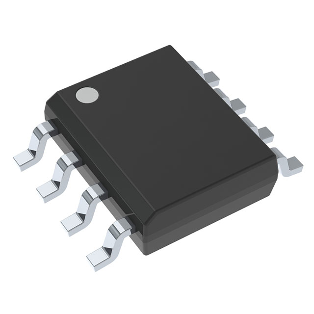
The OPA333AIDR is a high-performance operational amplifier (op-amp) designed and manufactured by Texas Instruments. It is part of the OP Amps, Buffer Amps ICs category and is known for its zero-drift performance. This IC op-amp features a single circuit within an 8-SOIC package, making it suitable for a wide range of applications that require precision and stability.
OPA333AIDR Features
- Voltage - Supply Span (Min/Max): The OPA333AIDR operates over a wide voltage range from 1.8 V to 5.5 V, providing flexibility in various power supply configurations.
- Gain Bandwidth Product: With a gain bandwidth product of 350 kHz, this op-amp offers a good balance between gain and speed, making it suitable for a variety of signal processing tasks.
- Slew Rate: A slew rate of 0.16V/µs ensures that the op-amp can handle fast-changing input signals without significant distortion.
- Current - Input Bias: The ultra-low input bias current of 70 pA contributes to the op-amp's high input impedance and low noise performance.
- Current - Supply: The quiescent supply current of 17 µA makes the OPA333AIDR energy-efficient, ideal for battery-powered applications.
- Voltage - Input Offset: The low input offset voltage of 2 µV ensures high accuracy and stability in circuit operation.
- Current - Output / Channel: Capable of sourcing or sinking up to 5 mA per channel, the OPA333AIDR can drive a variety of loads.
- Mounting Type: Surface mount technology allows for compact and reliable integration into printed circuit boards.
- REACH Status: REACH Unaffected ensures that the product is compliant with the European Union's Registration, Evaluation, Authorization, and Restriction of Chemicals (REACH) regulations.
- RoHS Status: ROHS3 Compliant means that the product is free from certain hazardous substances, making it environmentally friendly.
- Moisture Sensitivity Level (MSL): Rated at level 1, the OPA333AIDR is not sensitive to moisture, which simplifies handling and storage.
- ECCN: EAR99 indicates that the product is not subject to export controls under the U.S. Export Administration Regulations.
OPA333AIDR Applications
The OPA333AIDR is ideal for applications that require high precision and stability, such as:
- Sensor Conditioning: Its low drift and low noise make it suitable for conditioning signals from sensors in industrial and medical applications.
- Audio Amplification: The combination of low noise and high slew rate makes it an excellent choice for audio preamplifiers.
- Precision Instrumentation: The OPA333AIDR's low input offset voltage and low drift are beneficial in precision measurement and control systems.
- Data Acquisition Systems: Its wide supply voltage range and low power consumption make it suitable for battery-operated data acquisition systems.
Conclusion of OPA333AIDR
The OPA333AIDR from Texas Instruments stands out for its zero-drift performance, low noise, and wide supply voltage range. Its unique combination of technical specifications makes it an excellent choice for a variety of applications where precision and stability are paramount. Whether used in sensor conditioning, audio amplification, or precision instrumentation, the OPA333AIDR delivers reliable performance and meets stringent environmental and regulatory standards.
FAQ
| Quantity | Unit Price | Ext. Price |
|---|---|---|
| 10+ | $1.48628 | $14.86 |
| 30+ | $1.33715 | $40.11 |
| 100+ | $1.08857 | $108.86 |
| 500+ | $1.01315 | $506.57 |
| 1000+ | $0.98057 | $980.57 |
Not available to buy online? Want the lower wholesale price? Please Send RFQ to get best price, we will respond immediately


.png?x-oss-process=image/format,webp/resize,h_32)


