
Texas Instruments
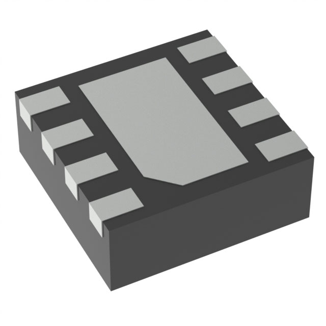
OPA855IDSGR
OP Amps, Buffer Amps ICs
OPA855IDSGR
687-OPA855IDSGR

Texas Instruments-OPA855IDSGR-datasheets-7029823.pdf
IC OPAMP GP 1 CIRCUIT 8WSON


- 1+
- $5.61218
- $5.61
- 10+
- $4.87361
- $48.74
- 30+
- $4.41655
- $132.5
- 100+
- $3.97440
- $397.44
ADD TO CART
QUICK ORDER
$5.61218
$5.61

.png?x-oss-process=image/format,webp/resize,p_30)


OPA855IDSGR Description
The OPA855IDSGR is a precision operational amplifier (op-amp) from Texas Instruments. It is designed for high accuracy and low noise applications, making it suitable for a wide range of uses.
Description:
The OPA855IDSGR is a single, precision operational amplifier that operates from a single supply voltage of 3.3V to 5.5V. It has a low input offset voltage of 1µV maximum and a low input bias current of 1pA maximum. The device also has a low noise level of 7nV/√Hz and a high output drive capability of ±100mA.
Features:
- Single supply operation from 3.3V to 5.5V
- Low input offset voltage: 1µV max
- Low input bias current: 1pA max
- Low noise level: 7nV/√Hz
- High output drive capability: ±100mA
- Precision operational amplifier
Applications:
The OPA855IDSGR is suitable for a wide range of applications that require high accuracy and low noise, including:
- Data acquisition systems
- Medical instrumentation
- Strain gauge amplifiers
- pH meter amplifiers
- Pressure sensor amplifiers
- Battery monitors
- Temperature measurement systems
- Audio equipment
- Industrial control systems
Overall, the OPA855IDSGR is a high-performance operational amplifier that offers excellent precision and low noise characteristics, making it ideal for use in a wide range of applications that demand high accuracy and low distortion.
Tech Specifications
Voltage - Supply Span (Max)
Number of Channels per Chip
Power Supply Type
Maximum Input Offset Voltage (mV)
Typical Output Current (mA)
PPAP
Gain Bandwidth Product
Product Status
Current - Input Bias
Automotive
Maximum Input Offset Current (uA)
Supplier Package
Package / Case
Typical Voltage Gain (dB)
REACH Status
Typical Input Bias Current (uA)
EU RoHS
Amplifier Type
Maximum Dual Supply Voltage (V)
Moisture Sensitivity Level (MSL)
Typical Input Noise Voltage Density (nV/rtHz)
Operating Temperature
Typical Slew Rate (V/us)
ECCN
Mounting Type
Current - Supply
Standard Package Name
Pin Count
Shut Down Support
Mounting
Minimum Single Supply Voltage (V)
Minimum PSRR (dB)
Typical Dual Supply Voltage (V)
Voltage - Supply Span (Min)
Lead Shape
Manufacturer Type
HTSUS
Package
Current - Output / Channel
Minimum CMRR (dB)
PCB changed
Output Type
HTS
ECCN (US)
Supplier Device Package
Minimum CMRR Range (dB)
Minimum Operating Temperature (°C)
Maximum Operating Temperature (°C)
Process Technology
Typical Gain Bandwidth Product (MHz)
Package Height
Mfr
RoHS Status
Maximum Input Bias Current (uA)
Typical Noninverting Input Current Noise Density (pA/rtHz)
-3db Bandwidth
Slew Rate
Package Length
Minimum Dual Supply Voltage (V)
Voltage - Input Offset
Series
Type
Maximum Single Supply Voltage (V)
Part Status
Number of Circuits
Package Width
Typical Settling Time (ns)
Base Product Number
Unit Weight
3 dB Bandwidth
en - Input Voltage Noise Density
Vos - Input Offset Voltage
Voltage Gain dB
Product
RoHS
Supply Voltage - Min
Operating Supply Current
SR - Slew Rate
Number of Channels
Features
Maximum Operating Temperature
Ib - Input Bias Current
Supply Voltage - Max
Mounting Style
PSRR - Power Supply Rejection Ratio
Minimum Operating Temperature
CMRR - Common Mode Rejection Ratio
In - Input Noise Current Density
Ios - Input Offset Current
Shutdown
Output Current per Channel
USHTS
GBP - Gain Bandwidth Product
OPA855IDSGR Documents
Download datasheets and manufacturer documentation for OPA855IDSGR
 Assembly 18/Sep/2023
  OPA855
  OPA855x 26/Jan/2023
 Shopping Guide

Payment Methods
Payment Methods include Prepayment TT (bank transfer), Western Union, and PayPal. Customers are responsible for shipping costs, bank charges, customs duties and taxes.


Shipping Rate
Shipments are made once a day around 5pm, excluding Sundays. Once shipped, the estimated delivery time is usually 5-7 business days, depending on the courier you choose.

Delivery Methods
Provide DHL, FedEx, UPS, EMS, SF Express and Registered Airmail International Delivery Service


.png?x-oss-process=image/format,webp/resize,h_32)


