
 German
 Japanese
 Portuguese
 Korea
Korea
 Mexico
 Dutch
Dutch


Texas Instruments
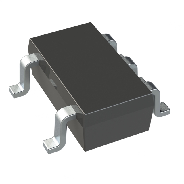
OPA990IDBVR

Why Choose Us?
Professional Platform
B2B & B2C purchasingDelivery at full speed
1-2 days deliveryWide variety
Original manufacturers365 days guarantee
Responsible quality
.png)


Tech Specifications
OPA990IDBVR Description
The Texas Instruments OPA990IDBVR is a high-performance, low-noise, and low-power operational amplifier (op-amp) designed for a wide range of applications. Here's a brief description of the model, its features, and potential applications:
Description:
The OPA990IDBVR is a member of the OPA990 family of operational amplifiers, which are designed to provide excellent DC and AC performance. The 'IDBVR' suffix indicates that the package is a 10-lead VSON (Very Small Outline, No Lead) package.
Features:
-
Low Input Noise: The OPA990IDBVR has a low input voltage noise of 5.2 nV/√Hz, making it suitable for applications where low-noise performance is critical.
-
Low Power Consumption: It operates with a low supply current of 2.2 mA per amplifier, which is beneficial for battery-powered or energy-sensitive applications.
-
Wide Supply Voltage Range: The device can operate with supply voltages from ±2.5V to ±18V, providing design flexibility.
-
High Input Impedance: It has a high input impedance of 1 pF to 10 pF, which is useful for driving capacitive loads without significant signal degradation.
-
High Output Current: The OPA990IDBVR can deliver up to ±600 mA output current, making it suitable for driving high-current loads.
-
Precision Performance: It offers precision characteristics such as low input offset voltage and drift, and low temperature coefficient, which are important for accurate signal processing.
-
Short Circuit Protection: The device includes internal protection against output short circuits.
-
Small Package Size: The VSON package is compact, making it suitable for space-constrained applications.
Applications:
-
Audio Applications: Due to its low noise and precision characteristics, the OPA990IDBVR is well-suited for high-fidelity audio amplifiers and preamplifiers.
-
Medical Instruments: Its low-noise performance makes it ideal for use in medical equipment that requires precise signal processing, such as ultrasound machines and patient monitoring systems.
-
Data Acquisition Systems: The precision and low-noise features are beneficial for data acquisition systems that require accurate signal conditioning.
-
Battery-Powered Devices: The low power consumption of the OPA990IDBVR makes it suitable for portable and battery-powered devices where energy efficiency is important.
-
Industrial Automation: It can be used in signal conditioning circuits for sensors and actuators in industrial control systems.
-
High-Current Drive Applications: The high output current capability makes it suitable for driving high-current loads, such as motor drivers or LED arrays.
-
Sensor Conditioning: The OPA990IDBVR can be used to condition signals from various types of sensors, including temperature, pressure, and humidity sensors.
-
Precision DC and AC Amplification: Its precision characteristics make it suitable for applications that require accurate amplification of both DC and AC signals.
The OPA990IDBVR is a versatile operational amplifier that can be used in a wide range of applications where low noise, precision, and low power consumption are important. Its compact package size also makes it suitable for applications with space constraints.
FAQ
| Quantity | Unit Price | Ext. Price |
|---|---|---|
| 10+ | $0.61885 | $6.19 |
| 30+ | $0.54172 | $16.25 |
| 100+ | $0.46628 | $46.63 |
| 500+ | $0.42172 | $210.86 |
| 1000+ | $0.39772 | $397.72 |
Not available to buy online? Want the lower wholesale price? Please Send RFQ to get best price, we will respond immediately


.png?x-oss-process=image/format,webp/resize,h_32)


