
Texas Instruments
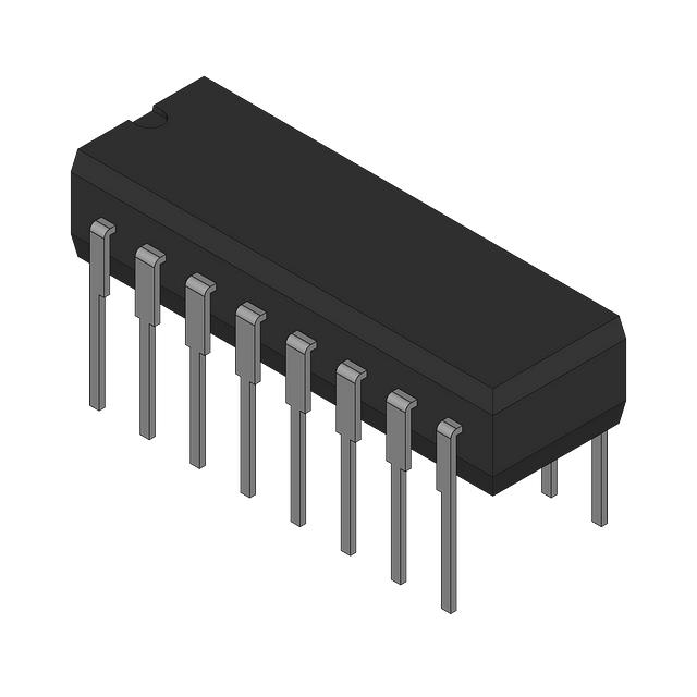
SN54LS109AJ
Flip Flops


.png?x-oss-process=image/format,webp/resize,p_30)


SN54LS109AJ Description
SN54LS109AJ Description
The SN54LS109AJ is a dual J-K positive-edge-triggered flip-flop designed by Texas Instruments, a leading manufacturer in the semiconductor industry. This logic IC chip is part of the 54LS109 family and is known for its robust performance and reliability. The device is categorized under Logic IC Chips and is ideal for a wide range of digital circuit applications.
The SN54LS109AJ features a dual J-K flip-flop configuration, which allows for versatile control and storage of binary data. Each flip-flop is triggered on the positive edge of the clock signal, ensuring precise timing and synchronization. This positive-edge triggering mechanism enhances the accuracy and reliability of data processing in digital systems.
SN54LS109AJ Features
- Dual J-K Flip-Flops: The SN54LS109AJ contains two independent J-K flip-flops, providing dual functionality in a single package. This dual configuration allows for efficient use of space and resources in complex digital circuits.
- Positive-Edge Triggering: The flip-flops are activated on the positive edge of the clock signal, ensuring precise timing and synchronization. This feature is crucial for applications requiring accurate data processing and control.
- High-Speed Operation: The SN54LS109AJ operates at high speeds, making it suitable for high-frequency digital systems. Its fast switching times and low propagation delays contribute to the overall performance of the circuit.
- Low Power Consumption: Designed with low power consumption in mind, the SN54LS109AJ is ideal for applications where energy efficiency is a priority. This feature helps in reducing power requirements and improving system efficiency.
- Active Product Status: The SN54LS109AJ is an active product, ensuring continued availability and support from Texas Instruments. This stability in product availability is crucial for long-term projects and maintenance.
- Bulk Packaging: Available in bulk packaging, the SN54LS109AJ is suitable for large-scale production and distribution. This packaging option ensures cost-effectiveness and ease of handling in manufacturing processes.
SN54LS109AJ Applications
The SN54LS109AJ is widely used in various digital circuit applications due to its versatile functionality and high performance. Some specific use cases include:
- Digital Counters: The dual J-K flip-flops can be used to build digital counters for counting and timing applications. The positive-edge triggering ensures accurate and reliable counting.
- Sequential Logic Circuits: The SN54LS109AJ is ideal for implementing sequential logic circuits, where the output depends on both the current input and the previous state. This makes it suitable for state machines and other control logic applications.
- Data Storage and Control: The flip-flops can be used for temporary data storage and control in digital systems. The dual configuration allows for efficient handling of binary data.
- Clock Synchronization: The positive-edge triggering mechanism makes the SN54LS109AJ suitable for clock synchronization applications, ensuring precise timing and coordination between different components of a digital system.
Conclusion of SN54LS109AJ
The SN54LS109AJ is a high-performance dual J-K positive-edge-triggered flip-flop from Texas Instruments, offering a range of technical specifications and performance benefits. Its dual flip-flop configuration, positive-edge triggering, high-speed operation, and low power consumption make it a versatile and reliable choice for various digital circuit applications. The active product status and bulk packaging further enhance its suitability for large-scale production and long-term projects. Whether used in digital counters, sequential logic circuits, data storage, or clock synchronization, the SN54LS109AJ provides a robust and efficient solution for digital systems.
Tech Specifications
SN54LS109AJ Documents
Download datasheets and manufacturer documentation for SN54LS109AJ
 JM38510/30109BEA Datasheet
 Shopping Guide


.png?x-oss-process=image/format,webp/resize,h_32)


