
Texas Instruments
SN74AC11N
Gates and Inverters


.png?x-oss-process=image/format,webp/resize,p_30)


SN74AC11N Description
SN74AC11N Description
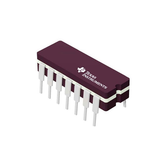
The SN74AC11N is a high-performance 3-input AND gate IC designed for a wide range of digital logic applications. Manufactured by Texas Instruments, this device belongs to the 74AC series, known for its high-speed operation and low power consumption. The SN74AC11N features a maximum propagation delay of 8ns at 5V with a load capacitance of 50pF, making it suitable for high-speed digital circuits. It operates within a supply voltage range of 2V to 6V and is available in a through-hole mounting package, specifically in a tube format.
The SN74AC11N is designed with three inputs and three circuits, providing flexibility in digital logic design. It has an input logic level low range of 0.9V to 1.65V and a high range of 2.1V to 3.85V, ensuring compatibility with various digital systems. The device offers a quiescent current of up to 2 µA and can handle output currents of up to 24mA for both high and low states. The SN74AC11N is REACH unaffected and RoHS3 compliant, adhering to environmental and safety standards.
SN74AC11N Features
- High-Speed Performance: With a maximum propagation delay of 8ns at 5V and 50pF, the SN74AC11N ensures rapid signal processing, making it ideal for high-speed digital circuits.
- Wide Operating Voltage Range: The device operates reliably within a supply voltage range of 2V to 6V, providing flexibility in power supply requirements.
- Low Power Consumption: The SN74AC11N features a quiescent current of only 2 µA, minimizing power usage and heat generation.
- High Output Current Capability: Capable of sourcing and sinking up to 24mA, the SN74AC11N can drive multiple loads efficiently.
- Environmental Compliance: The device is REACH unaffected and RoHS3 compliant, ensuring it meets stringent environmental and safety standards.
- Through-Hole Mounting: The through-hole package makes it suitable for applications requiring robust mechanical stability and ease of installation.
- Compatibility: The input logic levels are designed to be compatible with a wide range of digital systems, enhancing its versatility.
SN74AC11N Applications
The SN74AC11N is well-suited for a variety of applications where high-speed digital processing and low power consumption are critical. Some specific use cases include:
- Digital Logic Circuits: Ideal for complex digital systems requiring fast signal processing and low power consumption.
- Microcontroller Interfaces: Can be used to interface with microcontrollers, providing efficient signal conditioning and processing.
- Telecommunications: Suitable for high-speed data transmission and processing in telecom equipment.
- Automotive Electronics: The robust through-hole package and wide operating voltage range make it suitable for automotive applications.
- Industrial Control Systems: The device's high-speed performance and low power consumption make it ideal for industrial automation and control systems.
Conclusion of SN74AC11N
The SN74AC11N is a versatile and high-performance 3-input AND gate IC designed for demanding digital logic applications. Its combination of high-speed operation, low power consumption, and wide operating voltage range makes it a reliable choice for a variety of applications. The device's environmental compliance and robust through-hole package further enhance its appeal. Whether used in digital circuits, microcontroller interfaces, or industrial control systems, the SN74AC11N offers significant advantages over similar models, making it a preferred choice for engineers and designers in the electronics industry.
Tech Specifications
SN74AC11N Documents
Download datasheets and manufacturer documentation for SN74AC11N
 Mechanical Outline Drawing
  Add Cu as Alternative Bond Wire Metal for Select Devices (PDF) Product Change Notification (PDF) Product Change Notification_2024_09_03 (PDF)
  SN74AC11N Symbol & Footprint by SnapMagic
  Logic Guide (Rev. AB)
  SN74AC11 Behavioral SPICE Model
 Shopping Guide


.png?x-oss-process=image/format,webp/resize,h_32)


