Texas Instruments_SN74AUC1G74YZPR

Texas Instruments
SN74AUC1G74YZPR  
Flip Flops

Texas Instruments
SN74AUC1G74YZPR
706-SN74AUC1G74YZPR
Ersa
Texas Instruments-SN74AUC1G74YZPR-datasheets-5959056.pdf
IC FF D-TYPE SNGL 1BIT 8DSBGA
In Stock : 3198

Not available to buy online? Want the lower wholesale price? Please Send RFQ to get best price, we will respond immediately

QUICK RFQ
ADD TO RFQ LIST
ersa FreeSample ersa flow
  • Quantity
  • Unit Price
  • Ext. Price
    • 1+
    • $0.96710
    • $0.97
    • 10+
    • $0.94392
    • $9.44
    • 30+
    • $0.93067
    • $27.92
    ADD TO CART
    QUICK ORDER
    $0.96710    $0.97
    ISO9001
    Quality Policy
    ISO45001
    ISO14001

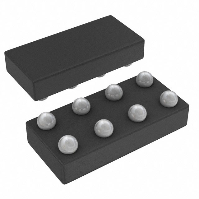
    SN74AUC1G74YZPR Description

    The SN74AUC1G74YZPR is a low-power silicon gate CMOS device manufactured by Texas Instruments. It is a dual D-type flip-flop with a clear (reset) input, designed for use in a wide range of digital applications.

    Description:

    The SN74AUC1G74YZPR is a dual D-type flip-flop, which means it consists of two separate flip-flops in a single package. Each flip-flop has a data input (D), a clock input (CLK), a clear (reset) input, and two outputs (Q and Q'). The clear input allows the flip-flops to be asynchronously reset to a known state.

    Features:

    1. Low power consumption: The device is designed to operate with a low power supply voltage, making it suitable for battery-powered applications.
    2. High noise immunity: The device has a high noise immunity, which means it can operate reliably in environments with high levels of electrical noise.
    3. Wide operating temperature range: The device can operate over a wide temperature range, making it suitable for use in a variety of environments.
    4. Small package size: The device is available in a small package, making it suitable for use in compact, space-constrained applications.

    Applications:

    The SN74AUC1G74YZPR has a wide range of applications in digital electronics, including:

    1. Data storage and transfer: The device can be used to store and transfer data in digital systems, such as computers and communication systems.
    2. Counters and frequency dividers: The device can be used to create counters and frequency dividers, which are used to count events or divide the frequency of a clock signal.
    3. Shift registers: The device can be used to create shift registers, which are used to store and shift data in digital systems.
    4. Latches and level detectors: The device can be used to create latches and level detectors, which are used to detect and hold a particular level of a signal.

    Overall, the SN74AUC1G74YZPR is a versatile and reliable device that can be used in a wide range of digital applications. Its low power consumption, high noise immunity, and small package size make it an ideal choice for use in compact, battery-powered systems.

    Tech Specifications

    Number of Channels per Chip
    Clock Frequency
    Unit Weight
    Maximum Propagation Delay Time @ Maximum CL (ns)
    PPAP
    Automotive
    RoHS
    Maximum High Level Output Current (mA)
    Absolute Propagation Delay Time (ns)
    REACH Status
    Triggering Type
    Output type
    Number of Element Outputs
    Maximum Operating Supply Voltage (V)
    Input Capacitance
    Max Propagation Delay @ V, Max CL
    Operating temperature range (°C)
    Supplier Temperature Grade
    Standard Package Name
    High Level Output Current
    Mounting
    Input Signal Type
    Typical Operating Supply Voltage (V)
    Package
    Clock frequency (max) (MHz)
    IOH (max) (mA)
    Maximum Quiescent Current (mA)
    Current - Output High, Low
    Output Type
    Trigger Type
    Process Technology
    Package Height
    Maximum Operating Temperature
    Width
    RoHS Status
    Number of channels
    Set/Reset
    Number of Input Lines
    Number of Element Inputs
    Maximum Low Level Output Current (mA)
    Minimum Operating Temperature
    Type
    Length
    Operating Supply Voltage
    Part Status
    Lead finish / Ball material
    Package Width
    Number of Circuits
    Supply voltage (min) (V)
    Product Status
    Supplier Package
    Package / Case
    Number of Channels
    Voltage - Supply
    Logic Function
    Number of Elements
    EU RoHS
    Carrier
    Moisture Sensitivity Level (MSL)
    Operating Temperature
    Logic Type
    ECCN
    MSL rating / Peak reflow
    Mounting Type
    Pin Count
    Lead Shape
    Quiescent Current
    Low Level Output Current
    HTSUS
    Pins
    USHTS
    Propagation Delay Time
    PCB changed
    HTS
    Number of Elements per Chip
    Rating
    ECCN (US)
    Supply current (max) (µA)
    Supplier Device Package
    Supply Voltage - Min
    Minimum Operating Temperature (°C)
    Maximum Operating Temperature (°C)
    Function
    Propagation Delay Test Condition (pF)
    Mfr
    Polarity
    Supply voltage (max) (V)
    Height
    Features
    Supply Voltage - Max
    Mounting Style
    Input Type
    Technology family
    Current - Quiescent (Iq)
    Number of Bits per Element
    Package Length
    REACH
    Series
    Input type
    Number of Output Lines
    IOL (max) (mA)
    Reset Type
    Bus Hold
    Logic Family
    Base Product Number
    Minimum Operating Supply Voltage (V)

    SN74AUC1G74YZPR Documents

    Download datasheets and manufacturer documentation for SN74AUC1G74YZPR

    Ersa Assembly Site 12/Oct/2023      
    Ersa SN74AUC1G74YZPR Datasheet      
    Ersa SN74AUC1G74YZPR Datasheet      

    Shopping Guide

    Payment Methods
    Payment Methods include Prepayment TT (bank transfer), Western Union, and PayPal. Customers are responsible for shipping costs, bank charges, customs duties and taxes.
    Shipping Rate
    Shipments are made once a day around 5pm, excluding Sundays. Once shipped, the estimated delivery time is usually 5-7 business days, depending on the courier you choose.
    Delivery Methods
    Provide DHL, FedEx, UPS, EMS, SF Express and Registered Airmail International Delivery Service