
Texas Instruments
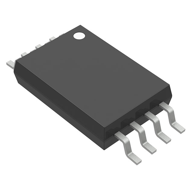
SN74CB3Q3305PWR
Encoders, Decoders, Multiplexers & Demultiplexers


.png?x-oss-process=image/format,webp/resize,p_30)


SN74CB3Q3305PWR Description
The Texas Instruments SN74CB3Q3305PWR is a 3-to-8 line decoder/demultiplexer integrated circuit (IC) that is designed to be used in digital electronic systems. Here is a description of the model, its features, and potential applications:
Model: SN74CB3Q3305PWR
Description:
The SN74CB3Q3305PWR is a high-performance 3-to-8 line decoder/demultiplexer that is part of the 74CB3Txx family of products. It is designed to be used in a wide range of digital applications, including data routing, signal distribution, and digital logic design.
Features:
- 3-to-8 Line Decoding: The device can take a 3-bit binary input and decode it into one of eight possible outputs, making it suitable for applications that require signal routing or distribution.
- Active-High Enable Input: The SN74CB3Q3305PWR features an active-high enable input, which allows the device to be turned on or off as needed.
- Low Power Consumption: The device is designed to operate with low power consumption, making it suitable for battery-powered or energy-sensitive applications.
- High-Speed Operation: The SN74CB3Q3305PWR is capable of high-speed operation, with a propagation delay of typically 3.5 ns (maximum 4.5 ns) and a minimum output rise and fall time of 1.5 ns (typical).
- 3-State Outputs: The outputs of the device are 3-state, which means they can be placed in a high-impedance state when not in use, allowing for daisy-chaining or multiplexing with other devices.
- Wide Operating Voltage Range: The device can operate over a wide range of supply voltages, from 1.65V to 5.5V, making it suitable for a variety of power supply configurations.
Applications:
- Data Routing: The SN74CB3Q3305PWR can be used to route data signals from a single source to one of multiple destinations based on the input code.
- Signal Distribution: In systems where multiple devices require the same input signal, the decoder can distribute the signal to the appropriate device.
- Digital Logic Design: The device can be used in the design of complex digital logic circuits, where signal routing and distribution are critical.
- Memory Address Decoding: In memory systems, the SN74CB3Q3305PWR can be used to decode address lines and select the appropriate memory location.
- I/O Expansion: The device can be used to expand the number of input/output lines in a microcontroller or other digital system, allowing for more complex control and interfacing.
The SN74CB3Q3305PWR is a versatile and high-performance device that can be used in a wide range of digital applications where signal routing, distribution, and decoding are required. Its low power consumption, high-speed operation, and wide operating voltage range make it a suitable choice for both portable and fixed installations.
Tech Specifications
SN74CB3Q3305PWR Documents
Download datasheets and manufacturer documentation for SN74CB3Q3305PWR
 SN74CB3Q3305
  SN74CB3Q3305
  Design 22/Feb/2022
 Shopping Guide


.png?x-oss-process=image/format,webp/resize,h_32)


