
 German
 Japanese
 Portuguese
 Korea
Korea
 Mexico
 Dutch
Dutch


Texas Instruments
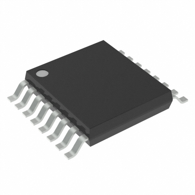
SN74HCS365QPWRQ1

Why Choose Us?
Professional Platform
B2B & B2C purchasingDelivery at full speed
1-2 days deliveryWide variety
Original manufacturers365 days guarantee
Responsible quality
.png)


Tech Specifications
SN74HCS365QPWRQ1 Description
The SN74HCS365QPWRQ1 is a 3.3V, 8-Input Multiplexer (MUX) from Texas Instruments. It is a high-speed Si-gate CMOS device that is designed to select one of eight analog or digital input signals and route it to a single output.
Description:
The SN74HCS365QPWRQ1 is a member of the 74HCxx family of CMOS devices. It is a 8-to-1 multiplexer, which means it can select one of eight input signals and route it to a single output. The device uses a 3-state design to prevent contention when the select inputs are changing.
Features:
- 3.3V operation
- 8-input multiplexer
- 3-state outputs
- High-speed Si-gate CMOS technology
- Wide operating temperature range (-40°C to +85°C)
- Low power consumption
- Available in a QFN package
Applications:
The SN74HCS365QPWRQ1 is suitable for a wide range of applications where signal selection is required. Some of the potential applications include:
- Digital signal processing systems
- Telecommunication systems
- Industrial control systems
- Audio/Video switching
- Medical equipment
- Automotive electronics
- Data acquisition systems
- Test and measurement equipment
In summary, the SN74HCS365QPWRQ1 is a versatile and reliable multiplexer that can be used in a variety of applications where signal selection is required. Its 3.3V operation, 3-state outputs, and low power consumption make it an ideal choice for many modern electronic systems.
FAQ
| Quantity | Unit Price | Ext. Price |
|---|---|---|
| 1+ | $0.88628 | $0.89 |
| 10+ | $0.72000 | $7.20 |
| 30+ | $0.63772 | $19.13 |
| 100+ | $0.55543 | $55.54 |
| 500+ | $0.50572 | $252.86 |
Not available to buy online? Want the lower wholesale price? Please Send RFQ to get best price, we will respond immediately


.png?x-oss-process=image/format,webp/resize,h_32)


