
 German
 Japanese
 Portuguese
 Korea
Korea
 Mexico
 Dutch
Dutch


Texas Instruments
SN74HCS367DR

Why Choose Us?
Professional Platform
B2B & B2C purchasingDelivery at full speed
1-2 days deliveryWide variety
Original manufacturers365 days guarantee
Responsible quality
.png)


Tech Specifications
SN74HCS367DR Description
SN74HCS367DR Description
The SN74HCS367DR is a high-performance, non-inverting buffer IC designed by Texas Instruments, belonging to the 74HCS series. This device is specifically engineered for applications requiring robust signal buffering and driving capabilities. The SN74HCS367DR features Schmitt trigger inputs, which provide excellent noise immunity and ensure stable operation even under varying input conditions. It supports a wide supply voltage range of 2V to 6V, making it versatile for different power supply environments.
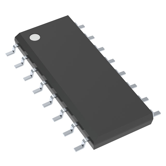
The SN74HCS367DR is packaged in a 16-pin SOIC (Small Outline Integrated Circuit) format, suitable for surface-mount technology (SMT) applications. This compact and reliable package is ideal for modern, space-constrained electronic designs. The device consists of two elements, each capable of handling 4 or 2 bits per element, offering flexibility in signal processing. The output current capabilities are rated at 7.8mA for both high and low states, ensuring strong drive capabilities for downstream circuits.
SN74HCS367DR Features
- Schmitt Trigger Inputs: Enhance noise immunity and provide stable operation under varying input conditions.
- Wide Supply Voltage Range: Operates efficiently between 2V and 6V, offering compatibility with a variety of power supply configurations.
- Non-Inverting Buffer: Preserves signal integrity and ensures reliable data transmission.
- Surface Mount Technology: Compatible with modern PCB assembly processes, ensuring ease of integration and high reliability.
- High Output Current Capability: 7.8mA for both high and low states, providing robust drive capabilities for downstream circuits.
- Moisture Sensitivity Level (MSL) 1: Unlimited storage time, reducing the risk of moisture-related failures during manufacturing.
- Active Product Status: Ensures long-term availability and support from Texas Instruments.
SN74HCS367DR Applications
The SN74HCS367DR is ideal for a variety of applications where signal buffering and driving are critical. Its robust design and wide voltage range make it suitable for:
- Digital Signal Processing: Enhances signal integrity in digital systems, ensuring reliable data transmission.
- Communication Interfaces: Provides stable buffering for data lines in various communication protocols.
- Embedded Systems: Ideal for buffering signals in microcontroller-based designs, ensuring reliable operation across different voltage levels.
- Automotive Electronics: Suitable for buffering signals in automotive control systems, where noise immunity and reliability are paramount.
- Industrial Automation: Enhances signal integrity in industrial control systems, ensuring robust operation in harsh environments.
Conclusion of SN74HCS367DR
The SN74HCS367DR from Texas Instruments is a versatile and reliable non-inverting buffer IC, offering significant advantages over similar models. Its Schmitt trigger inputs, wide supply voltage range, and high output current capabilities make it an excellent choice for applications requiring robust signal buffering and driving. The compact 16-pin SOIC package and surface-mount compatibility ensure ease of integration into modern electronic designs. Whether used in digital signal processing, communication interfaces, or industrial automation, the SN74HCS367DR delivers reliable performance and ensures stable operation in various environments.
FAQ
| Quantity | Unit Price | Ext. Price |
|---|---|---|
| 1+ | $0.43120 | $0.43 |
| 10+ | $0.30448 | $3.04 |
| 25+ | $0.27174 | $6.79 |
| 100+ | $0.23610 | $23.61 |
| 250+ | $0.21905 | $54.76 |
Not available to buy online? Want the lower wholesale price? Please Send RFQ to get best price, we will respond immediately


.png?x-oss-process=image/format,webp/resize,h_32)


