
 German
 Japanese
 Portuguese
 Korea
Korea
 Mexico
 Dutch
Dutch


Texas Instruments
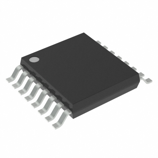
SN74HCS594PWR

Why Choose Us?
Professional Platform
B2B & B2C purchasingDelivery at full speed
1-2 days deliveryWide variety
Original manufacturers365 days guarantee
Responsible quality
.png)


Tech Specifications
SN74HCS594PWR Description
The SN74HCS594PWR is a high-performance, 8-bit serial-in, parallel-out shift register manufactured by Texas Instruments. This device is designed to be used in a variety of applications where data needs to be shifted and stored in parallel form. Here's a description of the model, its features, and potential applications:
Description:
The SN74HCS594PWR is a member of the 74HCxx family of logic devices, which are known for their high-speed performance and low power consumption. The device is a shift register that can be used to convert serial input data into parallel output data. It consists of an 8-stage shift register with a storage register for each bit and three-state outputs for easy interfacing with other devices.
Features:
- 8-bit Shift Register: The device has an 8-bit shift register that can store and shift data in a serial manner.
- Serial Input, Parallel Output: Data is input serially and output in parallel, making it suitable for applications requiring conversion between serial and parallel data formats.
- Three-State Outputs: The outputs can be placed in a high-impedance state (three-state), allowing for daisy-chaining or sharing of bus lines with other devices.
- Storage Register: Each bit has a corresponding storage register that can hold the shifted data.
- Master Reset: The device includes a master reset feature that clears all storage registers and the output latches.
- Clock Enable: A clock enable input allows for synchronous operation with other devices or systems.
- Clear: A clear input allows for asynchronous resetting of the shift register.
- Low Power Consumption: The device is designed for low power consumption, making it suitable for battery-powered or energy-sensitive applications.
- Wide Operating Voltage Range: It operates over a wide range of supply voltages, making it versatile for different power supply requirements.
Applications:
- LED Sequencing: Used to control the sequencing and brightness of LED displays in applications like advertising signs, traffic signals, and decorative lighting.
- Data Buffering: Acts as a buffer between serial data sources and parallel data sinks, such as in communication interfaces or data acquisition systems.
- Multiplexing: Utilized in multiplexing applications where multiple signals need to be time-division multiplexed onto a single communication line.
- Digital Clocks: Can be used to drive the digits and segments of digital clocks or other numeric displays.
- Control Systems: Used in control systems for managing the flow of digital signals, such as in robotics or industrial automation.
- Memory Address Latching: In memory systems, it can be used to latch address lines before accessing data.
- Telecommunication Equipment: Can be used in telecommunication equipment for signal processing and data formatting.
The SN74HCS594PWR is a versatile and reliable component that can be integrated into a wide range of digital systems requiring shift register functionality. Its combination of speed, low power consumption, and ease of interfacing makes it a popular choice for designers working with digital electronics.
FAQ
| Quantity | Unit Price | Ext. Price |
|---|---|---|
| 10+ | $0.42685 | $4.27 |
| 30+ | $0.37200 | $11.16 |
| 100+ | $0.32743 | $32.74 |
| 500+ | $0.31372 | $156.86 |
| 1000+ | $0.30515 | $305.15 |
Not available to buy online? Want the lower wholesale price? Please Send RFQ to get best price, we will respond immediately


.png?x-oss-process=image/format,webp/resize,h_32)


