
 German
 Japanese
 Portuguese
 Korea
Korea
 Mexico
 Dutch
Dutch


Texas Instruments
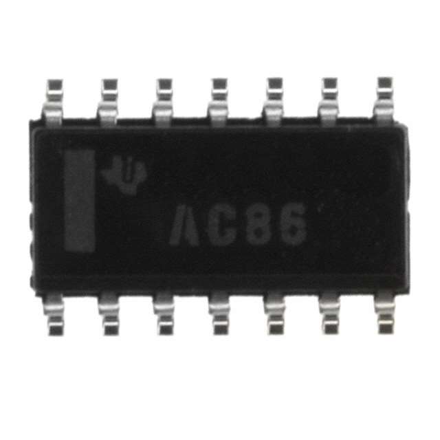
SN74LS06DBR

Why Choose Us?
Professional Platform
B2B & B2C purchasingDelivery at full speed
1-2 days deliveryWide variety
Original manufacturers365 days guarantee
Responsible quality
.png)


Tech Specifications
SN74LS06DBR Description
The SN74LS06DBR is a hex inverter gate integrated circuit (IC) manufactured by Texas Instruments. It is a part of the 74LSxx series of logic devices, which are low-power Schottky TTL (Transistor-Transistor Logic) integrated circuits. Here's a brief description, features, and applications of the SN74LS06DBR:
Description:
The SN74LS06DBR is a hex inverter gate, which means it contains six independent inverter gates in a single package. Each inverter gate takes a single binary input (0 or 1) and inverts it, producing the opposite binary output (1 or 0). The device is available in a SOIC (Small Outline Integrated Circuit) package, which is a common surface-mount package type.
Features:
- Hex inverter configuration: Six independent inverter gates in one package.
- Low-power Schottky TTL (LS) technology: Offers faster switching speeds and lower power consumption compared to standard TTL devices.
- Wide operating voltage range: It can operate with a supply voltage ranging from 2V to 6V, making it suitable for various applications.
- High noise immunity: The device is designed to operate reliably in noisy environments.
- RoHS compliant: The SN74LS06DBR is compliant with the Restriction of Hazardous Substances (RoHS) directive, which restricts the use of hazardous materials in electronic products.
Applications:
- Digital logic circuits: The SN74LS06DBR can be used to create various digital logic circuits, such as flip-flops, counters, and shift registers.
- Buffering: It can be used as a buffer to isolate or improve the signal quality in digital circuits.
- Signal inversion: The hex inverter configuration makes it suitable for applications where signal inversion is required.
- Logic level conversion: It can be used to convert logic levels between different digital systems or components.
- Educational purposes: The SN74LS06DBR is often used in educational settings to teach digital logic design and circuit analysis.
In summary, the SN74LS06DBR is a versatile hex inverter gate IC that offers a range of features, including low-power operation, high noise immunity, and a wide operating voltage range. It is suitable for various digital logic applications, buffering, signal inversion, and logic level conversion.
FAQ
| Quantity | Unit Price | Ext. Price |
|---|---|---|
| 1+ | $0.57257 | $0.57 |
| 10+ | $0.50057 | $5.01 |
| 30+ | $0.46457 | $13.94 |
| 100+ | $0.42857 | $42.86 |
Not available to buy online? Want the lower wholesale price? Please Send RFQ to get best price, we will respond immediately


.png?x-oss-process=image/format,webp/resize,h_32)


