
Texas Instruments
SN74LVC112ANSR
Flip Flops


.png?x-oss-process=image/format,webp/resize,p_30)


SN74LVC112ANSR Description
SN74LVC112ANSR Description
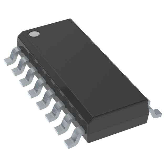
The SN74LVC112ANSR is a dual JK-type flip-flop integrated circuit (IC) designed by Texas Instruments, a leading manufacturer in the semiconductor industry. This IC is part of the 74LVC series, known for its robust performance and compatibility across a wide range of applications. The SN74LVC112ANSR features a clock frequency of up to 150 MHz, making it suitable for high-speed digital circuits. It operates within a supply voltage range of 1.65V to 3.6V, ensuring flexibility and compatibility with various power supply configurations.
SN74LVC112ANSR Features
- High-Speed Operation: With a maximum clock frequency of 150 MHz, the SN74LVC112ANSR ensures rapid data processing and signal handling, making it ideal for demanding digital applications.
- Complementary Outputs: The flip-flop provides complementary outputs, which can be used to drive both active-high and active-low signals, enhancing design flexibility.
- Negative Edge Triggering: The negative edge triggering mechanism ensures reliable and precise signal capture, minimizing timing errors and improving overall system reliability.
- Set and Reset Functionality: The IC includes set (preset) and reset functions, allowing for controlled initialization and clearing of flip-flop states, which is crucial for synchronous operations.
- Low Power Consumption: The SN74LVC112ANSR boasts a quiescent current of only 10 µA, making it energy-efficient and suitable for battery-powered and low-power applications.
- Wide Operating Voltage Range: The supply voltage range of 1.65V to 3.6V provides compatibility with various power supply systems, enhancing its versatility.
- Compliance and Reliability: The IC is REACH unaffected and RoHS3 compliant, ensuring it meets stringent environmental and safety standards. Additionally, its moisture sensitivity level (MSL) is 1 (unlimited), making it suitable for storage and handling in various environments.
- Surface Mount Packaging: The surface mount package (Tape & Reel) facilitates easy integration into modern PCB designs, ensuring efficient and reliable assembly processes.
SN74LVC112ANSR Applications
The SN74LVC112ANSR is well-suited for a variety of applications due to its high-speed operation, low power consumption, and versatile functionality. Some specific use cases include:
- Digital Signal Processing: The high clock frequency and negative edge triggering make it ideal for processing and synchronizing digital signals in communication systems and data processing units.
- Control Systems: The set and reset functions, along with complementary outputs, enable precise control and state management in microcontroller and microprocessor-based systems.
- Memory and Storage: The dual JK-type flip-flops can be used for memory elements and data storage applications, ensuring reliable data retention and retrieval.
- Consumer Electronics: The low power consumption and wide operating voltage range make it suitable for portable devices and consumer electronics where power efficiency and flexibility are critical.
- Industrial Automation: The robust performance and reliability of the SN74LVC112ANSR make it a reliable choice for industrial control systems and automation applications.
Conclusion of SN74LVC112ANSR
The SN74LVC112ANSR is a versatile and high-performance dual JK-type flip-flop IC that offers a combination of speed, efficiency, and reliability. Its unique features, such as negative edge triggering, complementary outputs, and low power consumption, provide significant advantages over similar models. The wide operating voltage range and compliance with environmental standards further enhance its appeal for a broad range of applications. Whether used in digital signal processing, control systems, or consumer electronics, the SN74LVC112ANSR is an excellent choice for engineers and designers seeking a reliable and efficient solution for their digital circuit needs.
Tech Specifications
SN74LVC112ANSR Documents
Download datasheets and manufacturer documentation for SN74LVC112ANSR
 SN74LVC112A
  SN74LVC112A
 Shopping Guide


.png?x-oss-process=image/format,webp/resize,h_32)


