
Texas Instruments
SN74LVC138AQPWREP
Encoders, Decoders, Multiplexers & Demultiplexers


.png?x-oss-process=image/format,webp/resize,p_30)


SN74LVC138AQPWREP Description
SN74LVC138AQPWREP Description
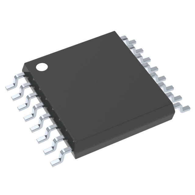
The SN74LVC138AQPWREP is a high-performance, 1 x 3:8 decoder/demultiplexer integrated circuit (IC) from Texas Instruments, designed for a wide range of digital applications. This IC is part of the 74LVC series, known for its low-voltage operation and compatibility with various CMOS and TTL logic families. The SN74LVC138AQPWREP features a single 3:8 decoding circuit, providing a versatile solution for address decoding and signal routing in digital systems.
SN74LVC138AQPWREP Features
- Low-Voltage Operation: The SN74LVC138AQPWREP operates within a voltage supply range of 2V to 3.6V, making it suitable for low-power applications and ensuring compatibility with modern digital systems.
- High Output Current: This IC can source and sink up to 24mA per output, providing robust performance in driving various loads.
- Single Supply Operation: Simplifies design by requiring only a single voltage supply source, reducing the need for multiple power rails.
- Surface Mount Technology (SMT): The surface mount package type facilitates easy integration into compact and high-density PCB designs.
- Compliance and Reliability: The SN74LVC138AQPWREP is REACH unaffected and RoHS3 compliant, ensuring environmental and regulatory compliance. It also has a moisture sensitivity level (MSL) of 1, making it suitable for unlimited storage conditions.
- Packaging: Available in tape and reel (TR) packaging, which is ideal for automated assembly processes and bulk handling.
SN74LVC138AQPWREP Applications
The SN74LVC138AQPWREP is ideal for a variety of applications where efficient signal decoding and demultiplexing are required. Some specific use cases include:
- Memory Address Decoding: Utilized in memory systems to decode address lines and select specific memory locations.
- Peripheral Control: Used in microcontroller and microprocessor systems to route control signals to various peripherals.
- Multiplexing and Demultiplexing: Ideal for applications requiring signal routing, such as in data acquisition systems and communication interfaces.
- Digital Logic Circuits: Employed in complex digital circuits to manage and distribute control signals efficiently.
Conclusion of SN74LVC138AQPWREP
The SN74LVC138AQPWREP from Texas Instruments offers a reliable and efficient solution for 1 x 3:8 decoding and demultiplexing tasks. Its low-voltage operation, high output current, and single supply requirement make it a versatile component for modern digital systems. The surface mount package and compliance with environmental regulations further enhance its suitability for a wide range of applications. Whether used in memory systems, peripheral control, or digital logic circuits, the SN74LVC138AQPWREP provides a robust and flexible solution for digital signal management.
Tech Specifications
SN74LVC138AQPWREP Documents
Download datasheets and manufacturer documentation for SN74LVC138AQPWREP
 Mechanical Outline Drawing
  Process Change Notification (PDF) Qualification of Mold Compound 4211471 and Mount Compound 4211470 for Select Devices Assembled in TI-Malaysia and TI-Taiwan using TSSOP package (PDF) Process Change notification (PDF)
  SN74LVC138AQPWREP Symbol & Footprint by SnapMagic
  Logic Guide (Rev. AB) Little Logic Guide 2018 (Rev. G)
 Shopping Guide


.png?x-oss-process=image/format,webp/resize,h_32)


