
Texas Instruments
SN74LVC14APWT
Gates and Inverters


.png?x-oss-process=image/format,webp/resize,p_30)


SN74LVC14APWT Description
SN74LVC14APWT Description
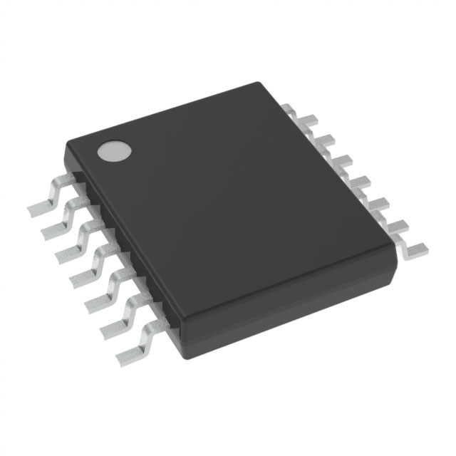
The SN74LVC14APWT is a high-performance, 6-channel inverter IC designed for a wide range of digital logic applications. Manufactured by Texas Instruments, this Surface Mount device belongs to the 74LVC series and is packaged in a 14-TSSOP format. It features a maximum propagation delay of 6.2ns at 3.3V with a 50pF load, ensuring fast signal processing and minimal latency. The SN74LVC14APWT operates within a supply voltage range of 1.65V to 3.6V, making it suitable for low-power applications. It also boasts low quiescent current (1 µA max) and high output current capabilities (24mA for both high and low states), which contribute to its energy efficiency and robust performance.
SN74LVC14APWT Features
- Logic Type: Inverter
- Number of Circuits: 6
- Number of Inputs: 1 per circuit
- Voltage - Supply: 1.65V to 3.6V
- Max Propagation Delay: 6.2ns @ 3.3V, 50pF
- Input Logic Levels: Low (0.15V to 0.8V), High (1.3V to 2V)
- Features: Schmitt Trigger
- Current - Quiescent (Max): 1 µA
- Current - Output High, Low: 24mA, 24mA
- Moisture Sensitivity Level (MSL): 1 (Unlimited)
- Mounting Type: Surface Mount
- Package: Tape & Reel (TR)
- ECCN: EAR99
- HTSUS: 8542.39.0001
- REACH Status: REACH Unaffected
- RoHS Status: ROHS3 Compliant
The SN74LVC14APWT's Schmitt Trigger feature ensures stable and reliable operation by providing hysteresis, which helps in filtering out noise and preventing unintended state changes. This makes it particularly advantageous in noisy environments or applications where signal integrity is critical.
SN74LVC14APWT Applications
The SN74LVC14APWT is ideal for a variety of applications due to its versatile operating voltage range, low power consumption, and high-speed performance. Some specific use cases include:
- Digital Signal Processing: The fast propagation delay and low quiescent current make it suitable for high-speed digital signal processing applications.
- Data Communication: Its robust output current capabilities and wide operating voltage range make it ideal for use in data communication systems where signal integrity is crucial.
- Consumer Electronics: The low power consumption and compact surface mount package make it a perfect fit for consumer electronics where space and energy efficiency are key considerations.
- Automotive Electronics: The high reliability and robust performance ensure it can withstand the demanding conditions often found in automotive applications.
Conclusion of SN74LVC14APWT
The SN74LVC14APWT is a versatile and high-performance inverter IC that offers significant advantages over similar models. Its fast propagation delay, low power consumption, and robust output capabilities make it suitable for a wide range of applications. The inclusion of Schmitt Trigger functionality ensures reliable operation in noisy environments, further enhancing its appeal. Whether used in digital signal processing, data communication, consumer electronics, or automotive applications, the SN74LVC14APWT provides a reliable and efficient solution for inverting digital signals.
Tech Specifications
SN74LVC14APWT Documents
Download datasheets and manufacturer documentation for SN74LVC14APWT
 SN54LVC14A, SN74LVC14A Logic Guide
  SN54LVC14A, SN74LVC14A Logic Guide
  Design 22/Feb/2022 SN74LVC14Ax 28/Apr/2022
 Shopping Guide


.png?x-oss-process=image/format,webp/resize,h_32)


