
 German
 Japanese
 Portuguese
 Korea
Korea
 Mexico
 Dutch
Dutch


Texas Instruments
SN74LVC1G04QDBVRQ1

Why Choose Us?
Professional Platform
B2B & B2C purchasingDelivery at full speed
1-2 days deliveryWide variety
Original manufacturers365 days guarantee
Responsible quality
.png)


Tech Specifications
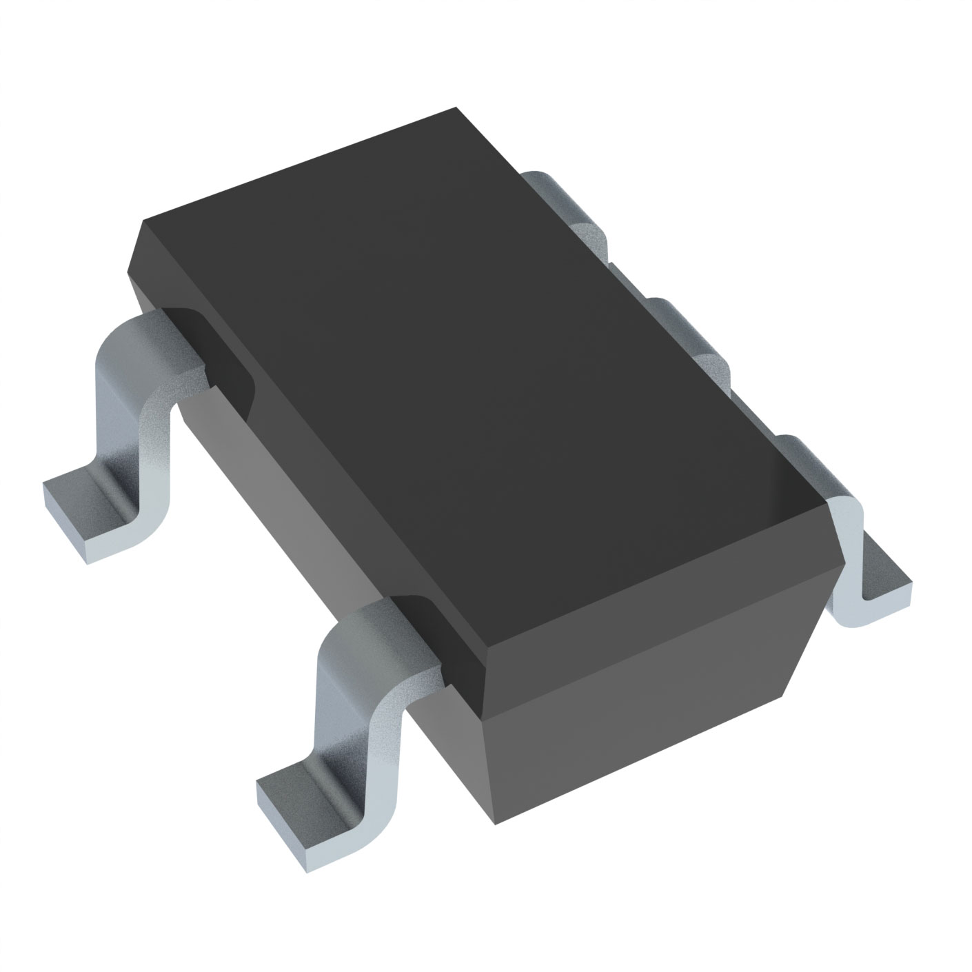
SN74LVC1G04QDBVRQ1 Description
The SN74LVC1G04QDBVRQ1 is a quad inverter gate manufactured by Texas Instruments. It is a part of the 74LVC1G04 series of logic gates, which are designed for low voltage and low power applications. Here is a description of the model, its features, and potential applications:
Description:
The SN74LVC1G04QDBVRQ1 is a member of the 74LVC1G04 series, which includes a range of low voltage logic gates. This particular model is a quad inverter gate, meaning it contains four independent inverter circuits within a single package. An inverter, also known as a NOT gate, takes a single binary input and produces a binary output that is the opposite of the input.
Features:
- Low Voltage Operation: The SN74LVC1G04QDBVRQ1 operates at a supply voltage range of 1.65V to 3.6V, making it suitable for applications where low power consumption is critical.
- Low Power Consumption: It is designed to consume minimal power, which is beneficial for battery-powered devices or systems where power efficiency is a priority.
- High Noise Immunity: The device has a high level of noise immunity, ensuring reliable operation even in environments with electrical noise.
- Small Package Size: It comes in a compact QFN (Quad Flat No-leads) package, which is ideal for space-constrained applications.
- Logic Level Compatibility: The SN74LVC1G04QDBVRQ1 is compatible with both TTL (Transistor-Transistor Logic) and CMOS (Complementary Metal-Oxide-Semiconductor) logic families, making it versatile for interfacing with different types of digital circuits.
Applications:
- Digital Circuit Design: The SN74LVC1G04QDBVRQ1 can be used in digital circuit design for inverting signals, buffering, or creating simple logic functions.
- Microcontroller Systems: It can be integrated into microcontroller systems to invert or buffer signals as needed.
- Automotive Electronics: Due to its low voltage and low power characteristics, the SN74LVC1G04QDBVRQ1 is suitable for automotive electronics where power efficiency and reliability are crucial.
- Portable Devices: It can be used in portable devices such as smartphones, tablets, and wearables, where power consumption and space are at a premium.
- Industrial Control Systems: The device can be utilized in industrial control systems for signal inversion and buffering, especially in applications where noise immunity is important.
In summary, the SN74LVC1G04QDBVRQ1 is a versatile quad inverter gate from Texas Instruments that offers low voltage operation, low power consumption, and high noise immunity in a compact package. It is suitable for a wide range of applications, from digital circuit design to portable devices and automotive electronics.
FAQ
| Quantity | Unit Price | Ext. Price |
|---|---|---|
| 5+ | $0.24581 | $1.23 |
| 50+ | $0.19244 | $9.62 |
| 150+ | $0.16957 | $25.44 |
| 500+ | $0.14104 | $70.52 |
Not available to buy online? Want the lower wholesale price? Please Send RFQ to get best price, we will respond immediately


.png?x-oss-process=image/format,webp/resize,h_32)


