
 German
 Japanese
 Portuguese
 Korea
Korea
 Mexico
 Dutch
Dutch


Texas Instruments
SN74LVC1G240DCKT

Why Choose Us?
Professional Platform
B2B & B2C purchasingDelivery at full speed
1-2 days deliveryWide variety
Original manufacturers365 days guarantee
Responsible quality
.png)


Tech Specifications
SN74LVC1G240DCKT Description
SN74LVC1G240DCKT Description
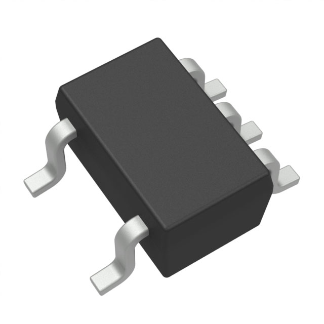
The SN74LVC1G240DCKT is a high-performance, single-bit inverting buffer IC designed for a wide range of digital applications. Manufactured by Texas Instruments, this device is part of the 74LVC series, known for its robustness and versatility. The SN74LVC1G240DCKT features a single inverting buffer element, making it ideal for signal inversion and buffering tasks. It operates over a wide supply voltage range of 1.65V to 5.5V, providing flexibility in power supply requirements. The device is available in a surface-mount SC70-5 package, which is compact and suitable for space-constrained designs. The SN74LVC1G240DCKT is RoHS3 compliant and REACH unaffected, ensuring it meets the latest environmental and regulatory standards.
SN74LVC1G240DCKT Features
- Single Inverting Buffer Element: The SN74LVC1G240DCKT provides a single inverting buffer, which is essential for applications requiring signal inversion.
- Wide Operating Voltage Range: With a supply voltage range of 1.65V to 5.5V, this IC can be used in various power supply environments, enhancing its versatility.
- High Output Current: The device supports an output current of 32mA for both high and low states, ensuring robust performance even under heavy load conditions.
- Surface-Mount Packaging: The SC70-5 package is compact and suitable for surface-mount technology (SMT), making it ideal for modern, space-efficient PCB designs.
- Environmental Compliance: The SN74LVC1G240DCKT is RoHS3 compliant and REACH unaffected, ensuring it meets stringent environmental regulations.
- Moisture Sensitivity Level (MSL) 1: The device has an unlimited moisture sensitivity level, making it suitable for a wide range of manufacturing processes without the need for special handling.
SN74LVC1G240DCKT Applications
The SN74LVC1G240DCKT is well-suited for a variety of applications due to its robust performance and wide operating voltage range. Some specific use cases include:
- Digital Signal Processing: The inverting buffer can be used to invert digital signals, which is crucial in many digital circuits.
- Microcontroller Interfaces: The device can interface with microcontrollers to manage signal inversion and buffering, ensuring reliable data transmission.
- Communication Systems: In communication systems, the SN74LVC1G240DCKT can be used to invert and buffer control signals, enhancing signal integrity.
- Consumer Electronics: The compact SC70-5 package makes it ideal for consumer electronics where space is limited, such as smartphones and tablets.
- Automotive Electronics: The wide voltage range and robust performance make it suitable for automotive applications where power supply variations are common.
Conclusion of SN74LVC1G240DCKT
The SN74LVC1G240DCKT is a versatile and reliable inverting buffer IC that offers significant advantages over similar models. Its wide operating voltage range, high output current, and compact surface-mount packaging make it suitable for a wide range of applications. The device's environmental compliance and unlimited moisture sensitivity level further enhance its appeal for modern electronics manufacturing. Whether used in digital signal processing, microcontroller interfaces, or consumer electronics, the SN74LVC1G240DCKT provides robust performance and reliability, making it an excellent choice for engineers and designers in the electronics industry.
FAQ
| Quantity | Unit Price | Ext. Price |
|---|---|---|
| 1+ | $0.73920 | $0.74 |
| 10+ | $0.52624 | $5.26 |
| 25+ | $0.47344 | $11.84 |
| 100+ | $0.41554 | $41.55 |
| 250+ | $0.38801 | $97.00 |
Not available to buy online? Want the lower wholesale price? Please Send RFQ to get best price, we will respond immediately


.png?x-oss-process=image/format,webp/resize,h_32)


