
Texas Instruments
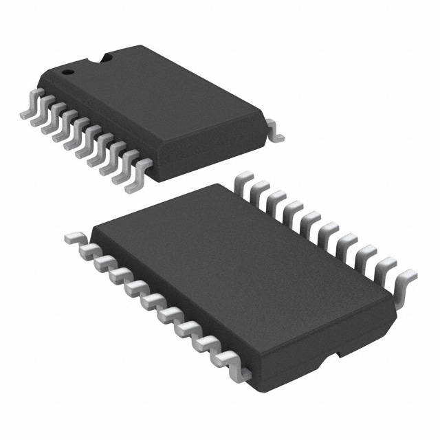
SN74LVC541ADW
Buffers, Drivers, Receivers, Transceivers

Not available to buy online? Want the lower wholesale price? Please Send RFQ to get best price, we will respond immediately


.png?x-oss-process=image/format,webp/resize,p_30)


SN74LVC541ADW Description
SN74LVC541ADW Description
The SN74LVC541ADW is a high-performance, 8-bit non-inverting buffer from Texas Instruments, designed for use in a wide range of electronic applications. This device is part of the 74LVC series and offers a supply voltage range of 1.65V to 3.6V, making it suitable for low-power systems. The SN74LVC541ADW is surface mountable, ensuring easy integration into modern electronic designs.
SN74LVC541ADW Features
- 8-Bit Non-Inverting Buffer: The SN74LVC541ADW provides an 8-bit non-inverting buffer, allowing for efficient signal transmission without signal inversion.
- Wide Supply Voltage Range: With a supply voltage range of 1.65V to 3.6V, this device is ideal for low-power applications.
- Surface Mount Technology: The surface mount design of the SN74LVC541ADW facilitates easy integration into modern electronic systems.
- High Output Current: Capable of sourcing and sinking 24mA, the SN74LVC541ADW can drive heavy loads with ease.
- RoHS Compliance: The SN74LVC541ADW is compliant with the RoHS3 directive, making it suitable for environmentally conscious applications.
- REACH Unaffected Status: This device is not affected by the REACH regulation, ensuring regulatory compliance in the European market.
SN74LVC541ADW Applications
The SN74LVC541ADW is ideal for a variety of applications where signal buffering is required without signal inversion. Some specific use cases include:
- Data Communication Systems: The SN74LVC541ADW can be used to buffer data signals in communication systems, ensuring reliable signal transmission.
- Industrial Control Systems: In industrial control systems, this device can be used to buffer control signals, improving system reliability and performance.
- Automotive Applications: The SN74LVC541ADW can be used in automotive applications where signal buffering is required, such as in infotainment systems or sensor interfaces.
- Low-Power Systems: Due to its low supply voltage range, this device is well-suited for low-power systems, such as battery-powered devices or energy-harvesting applications.
Conclusion of SN74LVC541ADW
The SN74LVC541ADW is a versatile, high-performance 8-bit non-inverting buffer from Texas Instruments. Its wide supply voltage range, high output current, and RoHS compliance make it an ideal choice for a variety of applications, including data communication systems, industrial control systems, automotive applications, and low-power systems. With its unique features and advantages over similar models, the SN74LVC541ADW is a reliable solution for buffering applications in the electronics industry.
Tech Specifications
SN74LVC541ADW Documents
Download datasheets and manufacturer documentation for SN74LVC541ADW
SN54LVC541A, SN74LVC541A SN54LVC541A, SN74LVC541A Material Set 21/Jun/2016 Related Parts


Shopping Guide


.png?x-oss-process=image/format,webp/resize,h_32)


©2025 ERSA Electronics Corporation.