Texas Instruments_SN74AUP1G125DRLR

Texas Instruments
SN74AUP1G125DRLR  
Buffers, Drivers, Receivers, Transceivers

Texas Instruments
SN74AUP1G125DRLR
704-SN74AUP1G125DRLR
Ersa
Texas Instruments-SN74AUP1G125DRLR-datasheets-530744.pdf
IC BUFFER NON-INVERT 3.6V SOT5
In Stock : 8865

Not available to buy online? Want the lower wholesale price? Please Send RFQ to get best price, we will respond immediately

QUICK RFQ
ADD TO RFQ LIST
ersa FreeSample ersa flow
  • Quantity
  • Unit Price
  • Ext. Price
    • 5+
    • $0.16785
    • $0.84
    • 50+
    • $0.13383
    • $6.69
    • 150+
    • $0.11722
    • $17.58
    • 500+
    • $0.10240
    • $51.2
    • 2500+
    • $0.09833
    • $245.82
    • 4000+
    • $0.09589
    • $383.56
    ADD TO CART
    QUICK ORDER
    $0.00000    $0.00
    ISO9001
    Quality Policy
    ISO45001
    ISO14001

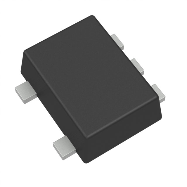
    SN74AUP1G125DRLR Description

    The SN74AUP1G125DRLR is a single-chip, high-speed, 3-state, non-inverting triple buffer/line driver gate manufactured by Texas Instruments. It is part of the 74AUP1G125 series, which is designed for low-power and high-speed applications.

    Description:

    The SN74AUP1G125DRLR is a member of the 74AUP1G125 series, which is a family of high-speed, low-power logic gates. The device is a triple buffer/line driver gate that provides non-inverting logic and 3-state outputs. It is available in a small-outline, surface-mount package (DRLR).

    Features:

    1. High-speed operation: The SN74AUP1G125DRLR is designed for high-speed applications, with a typical propagation delay of 3.5 ns.
    2. Low-power consumption: The device has a low power consumption of 3 mA per buffer, making it suitable for battery-powered or power-sensitive applications.
    3. 3-state outputs: The 3-state outputs allow for daisy-chaining multiple gates together, reducing the number of input pins required on the microcontroller or other control devices.
    4. Non-inverting logic: The device provides non-inverting logic, meaning that the output is the same as the input.
    5. Triple buffer/line driver: The SN74AUP1G125DRLR has three independent buffer/line driver gates, allowing for multiple signals to be buffered or driven simultaneously.
    6. Wide operating voltage range: The device operates over a wide voltage range of 1.65V to 5.5V, making it suitable for various applications and systems.

    Applications:

    1. Digital signal processing: The high-speed operation and low-power consumption make the SN74AUP1G125DRLR suitable for digital signal processing applications.
    2. Microcontroller I/O expansion: The 3-state outputs allow for easy expansion of microcontroller I/O pins, reducing the number of required pins and simplifying the design.
    3. Data communication: The device can be used in data communication systems, such as USB or serial communication interfaces, to buffer and drive signals.
    4. Display driving: The triple buffer/line driver can be used to drive multiple signals in LCD or LED displays, improving performance and reducing the load on the driving microcontroller.
    5. General-purpose buffering and signal conditioning: The SN74AUP1G125DRLR can be used in various applications where buffering, signal conditioning, or level conversion is required.

    In summary, the SN74AUP1G125DRLR is a high-speed, low-power, triple buffer/line driver gate from Texas Instruments, suitable for a wide range of applications, including digital signal processing, microcontroller I/O expansion, data communication, display driving, and general-purpose buffering.

    Tech Specifications

    Number of Channels per Chip
    Number of Output Enables per Chip
    Unit Weight
    Maximum Quiescent Current (uA)
    PPAP
    Automotive
    RoHS
    Maximum High Level Output Current (mA)
    Absolute Propagation Delay Time (ns)
    REACH Status
    Output type
    Maximum Operating Supply Voltage (V)
    Operating temperature range (°C)
    Standard Package Name
    High Level Output Current
    Mounting
    Input Signal Type
    Typical Operating Supply Voltage (V)
    Package
    IOH (max) (mA)
    Current - Output High, Low
    Output Type
    Supply Current - Max
    Process Technology
    Package Height
    Maximum Operating Temperature
    Width
    RoHS Status
    Number of channels
    Number of Inputs per Chip
    Number of Input Lines
    Maximum Low Level Output Current (mA)
    Minimum Operating Temperature
    Number of Input Enables per Chip
    Length
    Operating Supply Voltage
    Part Status
    Lead finish / Ball material
    Package Width
    Supply voltage (min) (V)
    Product Status
    Supplier Package
    Tradename
    Package / Case
    Number of Channels
    Technology
    Voltage - Supply
    Logic Function
    Number of Elements
    EU RoHS
    Carrier
    Moisture Sensitivity Level (MSL)
    Operating Temperature
    Tolerant I/Os (V)
    Logic Type
    ECCN
    MSL rating / Peak reflow
    Mounting Type
    Pin Count
    Lead Shape
    Quiescent Current
    Low Level Output Current
    HTSUS
    Pins
    USHTS
    Propagation Delay Time
    PCB changed
    HTS
    Number of Elements per Chip
    Rating
    ECCN (US)
    Supply current (max) (µA)
    Supplier Device Package
    Supply Voltage - Min
    Minimum Operating Temperature (°C)
    Maximum Operating Temperature (°C)
    Function
    Operating Supply Current
    Propagation Delay Test Condition (pF)
    Mfr
    Polarity
    Supply voltage (max) (V)
    Height
    Features
    Supply Voltage - Max
    Mounting Style
    Input Type
    Technology family
    Number of Bits per Element
    Number of Outputs per Chip
    Package Length
    REACH
    Series
    Input type
    Number of Output Lines
    IOL (max) (mA)
    Bus Hold
    Logic Family
    Base Product Number
    Minimum Operating Supply Voltage (V)

    SN74AUP1G125DRLR Documents

    Download datasheets and manufacturer documentation for SN74AUP1G125DRLR

    Ersa Mult Dev Assembly 14/Dec/2023      
    Ersa SN74AUP1G125YZTR      
    Ersa SN74AUP1G125YZTR      
    Ersa Die Conversion Revision A 19/Feb/2015       Die Conversion 09/Oct/2014      

    Shopping Guide

    Payment Methods
    Payment Methods include Prepayment TT (bank transfer), Western Union, and PayPal. Customers are responsible for shipping costs, bank charges, customs duties and taxes.
    Shipping Rate
    Shipments are made once a day around 5pm, excluding Sundays. Once shipped, the estimated delivery time is usually 5-7 business days, depending on the courier you choose.
    Delivery Methods
    Provide DHL, FedEx, UPS, EMS, SF Express and Registered Airmail International Delivery Service