
 German
 Japanese
 Portuguese
 Korea
Korea
 Mexico
 Dutch
Dutch


Texas Instruments
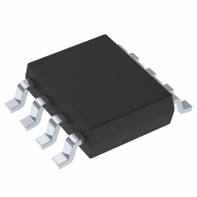
THS3062DDA

Why Choose Us?
Professional Platform
B2B & B2C purchasingDelivery at full speed
1-2 days deliveryWide variety
Original manufacturers365 days guarantee
Responsible quality
.png)


Tech Specifications
THS3062DDA Description
THS3062DDA Description
The THS3062DDA from Texas Instruments is a high-performance, dual-channel current feedback amplifier (CFA) designed for demanding high-speed signal processing applications. Packaged in an 8-SOP with PowerPAD, this active RoHS3-compliant IC operates over a 10V to 30V supply range, delivering exceptional bandwidth (2.2 GHz GBW, 300 MHz -3dB) and ultra-fast slew rate (7000 V/µs). Its current-feedback architecture ensures stable performance at high gains, making it ideal for video, RF, and precision analog systems. With low input bias current (6 µA) and high output drive (145 mA per channel), the THS3062DDA excels in driving low-impedance loads while maintaining signal integrity.
THS3062DDA Features
- High-Speed Performance: 2.2 GHz gain bandwidth and 7000 V/µs slew rate enable rapid signal amplification with minimal distortion.
- Wide Supply Range: Supports ±5V to ±15V dual supplies or 10V–30V single-supply operation for flexible design integration.
- Low Power Consumption: 8.3 mA supply current per channel balances speed and efficiency.
- Robust Output Drive: 145 mA output current per channel ensures stability into capacitive or resistive loads.
- Low Offset Voltage: 700 µV max minimizes DC errors in precision applications.
- Surface-Mount PowerPAD Package: Enhances thermal dissipation for reliability in compact designs.
THS3062DDA Applications
- High-Speed Signal Conditioning: Ideal for ADC/DAC buffers, RF amplifiers, and test equipment due to its wide bandwidth and low distortion.
- Video and Imaging Systems: Suitable for HD video drivers, CCD/CIS buffers, and cable/DSL line drivers.
- Communications Infrastructure: Used in baseband processing, optical transceivers, and active filters requiring high slew rates.
- Industrial and Medical Systems: Supports ultrasound, radar, and instrumentation where high-speed analog front-ends are critical.
Conclusion of THS3062DDA
The THS3062DDA stands out as a versatile, high-speed CFA amplifier, combining wide bandwidth, high slew rate, and robust output drive in a thermally efficient package. Its low power consumption and precision performance make it superior to traditional voltage-feedback amplifiers in high-frequency applications. Engineers can leverage its REACH-compliant, MSL1-rated design for reliable deployment in telecom, industrial, and medical systems demanding uncompromised signal fidelity.
FAQ
Not available to buy online? Want the lower wholesale price? Please Send RFQ to get best price, we will respond immediately


.png?x-oss-process=image/format,webp/resize,h_32)


