
Texas Instruments
THS3201D
OP Amps, Buffer Amps ICs


.png?x-oss-process=image/format,webp/resize,p_30)


THS3201D Description
THS3201D Description
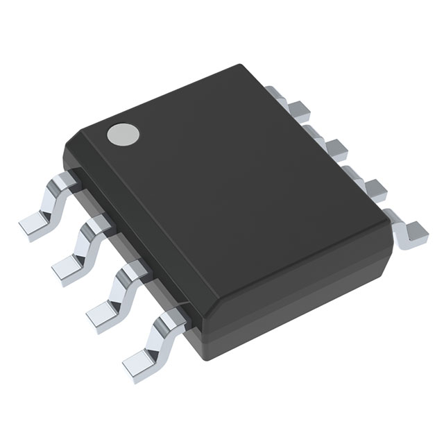
The THS3201D from Texas Instruments is a high-performance current feedback amplifier (CFA) designed for demanding high-speed applications. Packaged in an 8-SOIC form factor, this single-channel op-amp delivers exceptional bandwidth (1.8 GHz) and ultra-fast slew rate (9800 V/µs), making it ideal for signal conditioning, video processing, and RF systems. Operating over a 6.6V to 15V supply range, it features low input bias current (14 µA) and high output drive capability (115 mA per channel). Though marked as "Not For New Designs," it remains a robust choice for legacy or specialized systems requiring high-speed analog signal processing.
THS3201D Features
- Current Feedback Architecture: Enables superior bandwidth and slew rate performance compared to voltage-feedback amplifiers.
- High-Speed Performance: 1.8 GHz bandwidth and 9800 V/µs slew rate ensure minimal signal distortion in fast transient applications.
- Wide Supply Range: Supports 6.6V to 15V, accommodating various system requirements.
- Strong Output Drive: 115 mA output current allows direct driving of low-impedance loads.
- Low Input Offset Voltage: 700 µV enhances precision in DC-coupled circuits.
- Robust Packaging: 8-SOIC surface-mount package ensures reliability in compact designs.
- Compliance: ROHS3 Compliant and REACH Unaffected, meeting environmental standards.
THS3201D Applications
- High-Speed Signal Processing: Ideal for RF amplifiers, ADC drivers, and DAC buffers due to its wide bandwidth.
- Video and Imaging Systems: Suitable for HD video distribution, cable drivers, and CRT display circuits requiring fast signal fidelity.
- Test and Measurement Equipment: Enhances performance in oscilloscope front-ends and pulse generators.
- Communications Infrastructure: Used in broadband transceivers and optical networking for high-frequency signal integrity.
- Legacy System Maintenance: Despite its "Not For New Designs" status, it remains valuable for servicing existing high-speed analog systems.
Conclusion of THS3201D
The THS3201D stands out as a high-speed current feedback amplifier with exceptional bandwidth, slew rate, and output drive capabilities. While no longer recommended for new designs, its performance makes it a preferred choice for high-frequency analog systems, video processing, and precision test equipment. Engineers seeking a proven solution for fast signal amplification will find the THS3201D a reliable component, particularly in legacy or specialized applications where speed and stability are critical.
Tech Specifications
THS3201D Documents
Download datasheets and manufacturer documentation for THS3201D
 THS3201DGKR
  Design 25/Feb/2022
 Shopping Guide


.png?x-oss-process=image/format,webp/resize,h_32)


