
Texas Instruments
THS4012CD
OP Amps, Buffer Amps ICs


.png?x-oss-process=image/format,webp/resize,p_30)


THS4012CD Description
THS4012CD Description
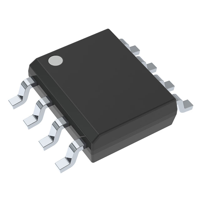
The THS4012CD is a high-performance, dual-channel voltage feedback operational amplifier designed for demanding applications requiring wide bandwidth and high slew rates. Manufactured by Texas Instruments, this IC is part of the OP Amps and Buffer Amps ICs category and is housed in an 8-pin SOIC package. The THS4012CD is ideal for applications that demand precision and high-speed signal processing, such as in high-frequency communication systems, video signal processing, and high-speed data acquisition systems.
THS4012CD Features
- Wide Supply Voltage Range: The THS4012CD operates with a supply voltage range from 9V to 32V, making it suitable for a variety of power supply configurations.
- High Gain Bandwidth Product: With a gain bandwidth product of 290 MHz, the THS4012CD ensures high-frequency performance and stability, making it ideal for applications requiring wide bandwidth.
- High Slew Rate: The 310V/µs slew rate enables the THS4012CD to handle high-frequency signals with minimal distortion, ensuring precise signal reproduction.
- Low Input Bias Current: The low input bias current of 2 µA minimizes the impact of input leakage currents on the signal, enhancing the accuracy of the amplifier.
- Low Input Offset Voltage: The 1 mV input offset voltage ensures high accuracy in signal processing, making the THS4012CD suitable for precision applications.
- High Output Current: Each channel can deliver up to 110 mA of output current, providing robust performance even under heavy load conditions.
- Surface Mount Technology: The surface mount package type facilitates easy integration into compact and high-density PCB designs.
- Operating Temperature Range: The THS4012CD operates within a temperature range of 0°C to 70°C, ensuring reliable performance in a variety of environmental conditions.
- Compliance and Reliability: The THS4012CD is REACH unaffected and RoHS3 compliant, ensuring environmental safety and reliability. It also has a moisture sensitivity level (MSL) of 1 (unlimited), making it suitable for various manufacturing processes.
THS4012CD Applications
The THS4012CD is well-suited for a range of applications due to its high performance and versatility:
- High-Speed Signal Processing: Ideal for applications requiring high-frequency signal processing, such as in communication systems and radar signal processing.
- Video Signal Processing: The wide bandwidth and high slew rate make the THS4012CD suitable for video signal amplification and processing, ensuring high-quality video output.
- Data Acquisition Systems: The high precision and low offset voltage make it ideal for high-speed data acquisition systems, where accurate signal reproduction is critical.
- Industrial Automation: The robust performance and high output current make the THS4012CD suitable for industrial automation applications, where reliable and precise signal processing is required.
Conclusion of THS4012CD
The THS4012CD from Texas Instruments is a high-performance dual-channel voltage feedback operational amplifier that offers a combination of wide bandwidth, high slew rate, and low input bias current. Its versatile supply voltage range, low input offset voltage, and high output current make it suitable for a variety of demanding applications. The THS4012CD's compliance with environmental standards and its surface mount package type further enhance its suitability for modern, compact electronic designs. Whether used in high-speed communication systems, video signal processing, or data acquisition systems, the THS4012CD delivers reliable and precise performance, making it a standout choice in its category.
Tech Specifications
THS4012CD Documents
Download datasheets and manufacturer documentation for THS4012CD
 THS4011CDG4
  THS4011CDG4
  Design 25/Feb/2022
 Shopping Guide


.png?x-oss-process=image/format,webp/resize,h_32)


