
 German
 Japanese
 Portuguese
 Korea
Korea
 Mexico
 Dutch
Dutch


Texas Instruments
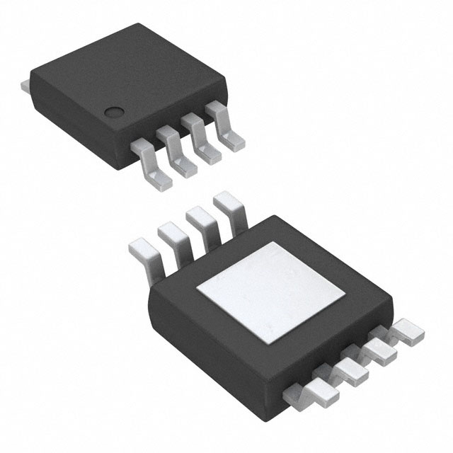
THS4131IDGNG4

Why Choose Us?
Professional Platform
B2B & B2C purchasingDelivery at full speed
1-2 days deliveryWide variety
Original manufacturers365 days guarantee
Responsible quality
.png)


Tech Specifications
THS4131IDGNG4 Description
THS4131IDGNG4 Description
The THS4131IDG4NG is a high-performance differential operational amplifier from Texas Instruments, designed for applications requiring high-speed signal processing and precision performance. This single-circuit op-amp features a wide supply voltage range of 4 V to 33 V, making it suitable for a variety of power supply configurations. The device offers a differential output type, which is ideal for applications where balanced signal transmission and noise rejection are critical.
THS4131IDGNG4 Features
- Wide Supply Voltage Range: Operates from 4 V to 33 V, providing flexibility in power supply design.
- High Gain Bandwidth Product: Achieves a gain bandwidth product of 225 MHz, ensuring high-frequency performance and fast signal processing.
- High Slew Rate: A slew rate of 52 V/µs enables the amplifier to handle high-frequency signals with minimal distortion.
- Low Input Bias Current: With an input bias current of only 2 µA, the THS4131IDGNG4 minimizes the impact on sensitive input sources.
- Low Input Offset Voltage: An input voltage offset of 200 µV ensures high precision in signal amplification.
- High Output Current: Capable of delivering up to 85 mA per channel, making it suitable for driving high-load applications.
- Surface Mount Packaging: The 8HVSSOP package is designed for surface mount technology, facilitating easy integration into compact PCB designs.
- Compliance and Reliability: The device is REACH unaffected and RoHS3 compliant, ensuring environmental and regulatory compliance. It also has a moisture sensitivity level (MSL) of 1, making it suitable for a wide range of manufacturing environments.
THS4131IDGNG4 Applications
The THS4131IDGNG4 is well-suited for a variety of high-speed and high-precision applications, including:
- High-Speed Signal Processing: Ideal for applications requiring and fast accurate signal amplification and processing, such as in high-speed data acquisition systems.
- Precision Instrumentation: Suitable for precision measurement equipment where low offset voltage and low bias current are critical.
- Communication Systems: The differential output type and high slew rate make it ideal for communication systems requiring balanced signal transmission and high-frequency operation.
- Medical Equipment: The high performance and reliability of the THS4131IDGNG4 make it suitable for medical devices where precision and speed are paramount.
Conclusion of THS4131IDGNG4
The THS4131IDGNG4 from Texas Instruments stands out as a versatile and high-performance differential operational amplifier. Its wide supply voltage range, high gain bandwidth product, and high slew rate make it suitable for a variety of demanding applications. The low input bias current and low input offset voltage ensure precision in signal processing, while the high output current capability allows it to drive heavy loads. The device's compliance with environmental and regulatory standards, along with its surface mount packaging, make it an excellent choice for modern electronic designs. Whether used in high-speed data acquisition, precision instrumentation, communication systems, or medical equipment, the THS4131IDGNG4 offers superior performance and reliability, making it a preferred choice for engineers and designers in the electronics. industry
FAQ
Not available to buy online? Want the lower wholesale price? Please Send RFQ to get best price, we will respond immediately


.png?x-oss-process=image/format,webp/resize,h_32)


