
 German
 Japanese
 Portuguese
 Korea
Korea
 Mexico
 Dutch
Dutch


Texas Instruments
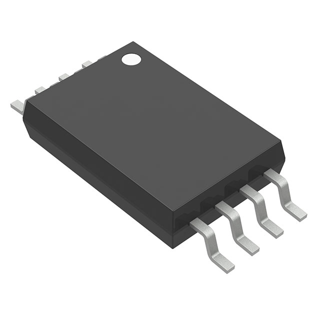
TL082CPW

Why Choose Us?
Professional Platform
B2B & B2C purchasingDelivery at full speed
1-2 days deliveryWide variety
Original manufacturers365 days guarantee
Responsible quality
.png)


Tech Specifications
TL082CPW Description
TL082CPW Description
The TL082CPW is a dual JFET operational amplifier designed for a wide range of applications requiring high input impedance and low noise performance. Manufactured by Texas Instruments, this IC is housed in an 8-lead TSSOP package, making it suitable for surface mount applications. The TL082CPW offers a maximum supply voltage range of 30 V and a minimum supply voltage range of 10 V, providing flexibility in power supply requirements. It features a gain bandwidth product of 3 MHz and a slew rate of 13 V/µs, ensuring high-frequency performance and fast transient response.
TL082CPW Features
- High Input Impedance: The TL082CPW utilizes JFET input transistors, resulting in an extremely high input impedance of 1 TΩ and a low input bias current of 30 pA. This makes it ideal for applications where signal integrity is crucial.
- Wide Supply Voltage Range: With a supply voltage range of 10 V to 30 V, the TL082CPW can operate in a variety of power supply configurations, enhancing its versatility.
- Low Noise Performance: The operational amplifier is designed to provide low noise characteristics, making it suitable for precision signal processing applications.
- High Slew Rate: The 13 V/µs slew rate ensures that the TL082CPW can handle fast-changing signals without significant distortion.
- Dual Channel Design: The TL082CPW features two independent operational amplifier circuits, allowing for multiple signal processing tasks within a single package.
- Low Input Offset Voltage: The input offset voltage is as low as 3 mV, which is critical for maintaining accuracy in precision applications.
- Compliance and Reliability: The TL082CPW is REACH unaffected and ROHS3 compliant, ensuring it meets environmental and regulatory standards. Additionally, it has a moisture sensitivity level (MSL) of 1, making it suitable for unlimited storage conditions.
TL082CPW Applications
The TL082CPW is well-suited for a variety of applications due to its high input impedance, low noise, and wide supply voltage range. Some specific use cases include:
- Precision Signal Amplification: Ideal for applications requiring high input impedance and low noise, such as in medical equipment, precision instrumentation, and low-level signal processing.
- Audio Processing: The TL082CPW's high slew rate and low noise make it suitable for audio amplifiers and preamplifiers, ensuring high-fidelity sound reproduction.
- Analog Signal Processing: Its dual-channel design allows for efficient processing of multiple analog signals, making it useful in multi-channel data acquisition systems and control circuits.
- Industrial Automation: The wide supply voltage range and robust performance make it suitable for industrial applications where reliability and precision are paramount.
Conclusion of TL082CPW
The TL082CPW is a versatile dual JFET operational amplifier that offers high input impedance, low noise, and a wide supply voltage range. Its dual-channel design, low input offset voltage, and high slew rate make it suitable for a variety of precision applications. Despite being marked as obsolete, the TL082CPW remains a reliable choice for applications requiring high performance and precision. Its compliance with environmental and regulatory standards ensures its suitability for modern electronics design.
FAQ
Not available to buy online? Want the lower wholesale price? Please Send RFQ to get best price, we will respond immediately


.png?x-oss-process=image/format,webp/resize,h_32)


