

Texas Instruments
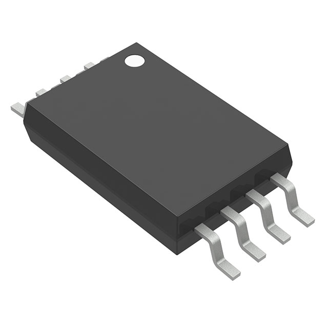
TLC2252CPW
OP Amps, Buffer Amps ICs

Not available to buy online? Want the lower wholesale price? Please Send RFQ to get best price, we will respond immediately


.png?x-oss-process=image/format,webp/resize,p_30)


TLC2252CPW Description
TLC2252CPW Description
The TLC2252CPW is a general-purpose operational amplifier from Texas Instruments, featuring a dual-channel design in an 8-pin TSSOP package. This IC is part of the LinCMOS™ series, known for its robust performance and versatility. Despite being marked as obsolete, the TLC2252CPW remains a reliable choice for applications requiring low power consumption and high input impedance.
TLC2252CPW Features
- Supply Voltage Range: The TLC2252CPW operates within a supply voltage range of 4.4 V to 16 V, making it suitable for a wide range of power supply configurations.
- Gain Bandwidth Product: With a gain bandwidth product of 210 kHz, this op-amp offers a balance between gain and frequency response, ideal for moderate-speed applications.
- Low Input Bias Current: The extremely low input bias current of 1 pA ensures minimal loading on the input signal source, preserving signal integrity.
- Low Offset Voltage: A voltage input offset of 200 µV ensures high accuracy in signal processing, making it suitable for precision applications.
- Slew Rate: The 0.12 V/µs slew rate provides stable performance in applications requiring moderate signal slew rates.
- Power Consumption: The low supply current of 80 µA (per channel) makes this op-amp highly energy-efficient, suitable for battery-powered and low-power applications.
- Output Current Capability: Each channel can deliver up to 50 mA of output current, providing robust performance for driving various loads.
- Operating Temperature Range: The TLC2252CPW operates within a temperature range of 0°C to 70°C, ensuring reliable performance in standard industrial environments.
- Compliance and Packaging: The TLC2252CPW is REACH unaffected and RoHS3 compliant, ensuring environmental and regulatory compliance. It is packaged in a tube, facilitating easy handling and storage.
TLC2252CPW Applications
The TLC2252CPW is well-suited for a variety of applications due to its general-purpose nature and robust performance characteristics. Some specific use cases include:
- Signal Conditioning: Ideal for amplifying and conditioning weak signals in sensor interfaces and data acquisition systems.
- Analog Filters: Suitable for designing active filters that require moderate bandwidth and low power consumption.
- Transimpedance Amplifiers: The low input bias current makes it suitable for applications where high input impedance is crucial, such as in photodiode circuits.
- Precision Measurement: The low offset voltage and high input impedance make it suitable for precision measurement applications, such as in medical equipment and scientific instruments.
- Battery-Powered Devices: The low power consumption and wide supply voltage range make it an excellent choice for battery-powered devices and portable electronics.
Conclusion of TLC2252CPW
The TLC2252CPW from Texas Instruments is a versatile general-purpose operational amplifier that offers a balance of performance and power efficiency. Despite its obsolete status, its low power consumption, high input impedance, and moderate gain bandwidth product make it a reliable choice for a wide range of applications. The TLC2252CPW is particularly well-suited for applications requiring precision signal processing, low power consumption, and moderate bandwidth. Its compliance with environmental and regulatory standards ensures its suitability for modern electronics design.
Tech Specifications
TLC2252CPW Documents
Download datasheets and manufacturer documentation for TLC2252CPW
TLC225x, TLC225xA Mult Dev EOL 7/Sep/2023 Related Parts


Shopping Guide


.png?x-oss-process=image/format,webp/resize,h_32)


©2025 ERSA Electronics Corporation.