
 German
 Japanese
 Portuguese
 Korea
Korea
 Mexico
 Dutch
Dutch


Texas Instruments
TLC2252IP

Why Choose Us?
Professional Platform
B2B & B2C purchasingDelivery at full speed
1-2 days deliveryWide variety
Original manufacturers365 days guarantee
Responsible quality
.png)


Tech Specifications
TLC2252IP Description
TLC2252IP Description
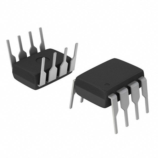
The TLC2252IP from Texas Instruments is a dual-channel general-purpose operational amplifier from the LinCMOS™ series, designed for precision analog applications. Housed in an 8-pin DIP (Through Hole) package, it operates over a wide supply voltage range of 4.4V to 16V, making it versatile for both low and higher voltage designs. With an ultra-low input bias current of 1 pA and a low input offset voltage of 200 µV, it ensures high accuracy in signal conditioning. The device is RoHS3 compliant and REACH unaffected, meeting stringent environmental standards.
TLC2252IP Features
- Low Power Consumption: Only 80µA per channel supply current, ideal for battery-powered systems.
- High Precision: 1 pA input bias current and 200 µV offset voltage minimize errors in sensitive circuits.
- Moderate Speed: 210 kHz gain bandwidth and 0.12V/µs slew rate suit low-frequency signal processing.
- Robust Output Drive: 50 mA output current per channel enables driving heavier loads.
- Wide Supply Range: 4.4V to 16V operation supports diverse power configurations.
- Reliable Packaging: Through-hole DIP ensures easy prototyping and rugged assembly.
TLC2252IP Applications
- Sensor Signal Conditioning: Ideal for amplifying low-level signals from thermocouples, strain gauges, and pressure sensors.
- Portable & Battery-Powered Devices: Low current draw makes it perfect for medical instruments, handheld meters, and IoT sensors.
- Active Filters & Integrators: Suited for low-frequency analog filtering due to its stable bandwidth.
- Precision Voltage References: Used in ADC/DAC buffer circuits where accuracy is critical.
- Industrial Control Systems: Reliable performance in process control and instrumentation environments.
Conclusion of TLC2252IP
The TLC2252IP stands out for its ultra-low power consumption, high precision, and robust design, making it a top choice for low-frequency, high-accuracy analog applications. Its wide supply range and strong output drive enhance versatility, while the through-hole package ensures ease of use in prototyping. Whether in portable electronics, industrial systems, or sensor interfaces, this op-amp delivers reliable performance with minimal power overhead.
FAQ
Not available to buy online? Want the lower wholesale price? Please Send RFQ to get best price, we will respond immediately


.png?x-oss-process=image/format,webp/resize,h_32)


