
Texas Instruments
TLC2262CD
OP Amps, Buffer Amps ICs


.png?x-oss-process=image/format,webp/resize,p_30)


TLC2262CD Description
TLC2262CD Description
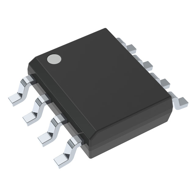
The TLC2262CD from Texas Instruments is a dual-channel CMOS operational amplifier (op-amp) belonging to the LinCMOS™ series. Packaged in an 8-SOIC tube, it is designed for precision analog applications requiring low power consumption and high input impedance. Operating within a 4.4V to 16V supply range, it delivers a 730 kHz gain bandwidth product (GBW) and a 0.55V/µs slew rate, making it suitable for moderate-speed signal conditioning. With an ultra-low 1 pA input bias current and 300 µV input offset voltage, it excels in high-impedance sensor interfaces and battery-powered systems. The device is RoHS3 compliant, REACH unaffected, and rated for 0°C to 70°C operation, ensuring reliability in industrial and consumer applications.
TLC2262CD Features
- Low Power Consumption: 425µA per channel supply current, ideal for portable and battery-operated devices.
- High Input Impedance: CMOS technology enables 1 pA input bias current, minimizing loading effects in high-Z circuits.
- Wide Supply Range: 4.4V to 16V operation supports diverse power configurations.
- Moderate Speed: 730 kHz GBW and 0.55V/µs slew rate balance performance and power efficiency.
- Robust Output: 50 mA output current per channel drives capacitive loads or small transducers.
- Reliable Packaging: 8-SOIC surface-mount package with MSL 1 (Unlimited) moisture sensitivity.
TLC2262CD Applications
- Sensor Signal Conditioning: Ideal for piezoelectric, thermocouple, or photodiode interfaces due to low input bias current.
- Active Filters: GBW and slew rate suit 2nd-order LP/HP filters in audio or instrumentation systems.
- Battery-Powered Systems: Low quiescent current extends runtime in IoT nodes, wearables, and medical devices.
- Portable Test Equipment: Combines precision and power efficiency for handheld multimeters or data loggers.
- Industrial Control: Stable performance in 0°C to 70°C environments for process monitoring or actuator drives.
Conclusion of TLC2262CD
The TLC2262CD stands out for its ultra-low input bias current, wide voltage range, and CMOS-based precision, making it a versatile choice for low-power, high-impedance applications. Its balance of speed, power efficiency, and robustness suits sensor interfaces, portable electronics, and industrial systems where reliability and performance are critical. Texas Instruments' LinCMOS™ technology ensures consistent quality, while RoHS3 compliance aligns with modern environmental standards. For designers seeking a cost-effective, dual-channel op-amp with minimal power drain, the TLC2262CD is a compelling solution.
Tech Specifications
TLC2262CD Documents
Download datasheets and manufacturer documentation for TLC2262CD
 TLC226x, TLC226xA
  Mult Devices Font 21/Apr/2018 Design 25/Feb/2022
 Shopping Guide


.png?x-oss-process=image/format,webp/resize,h_32)


