
 German
 Japanese
 Portuguese
 Korea
Korea
 Mexico
 Dutch
Dutch


Texas Instruments
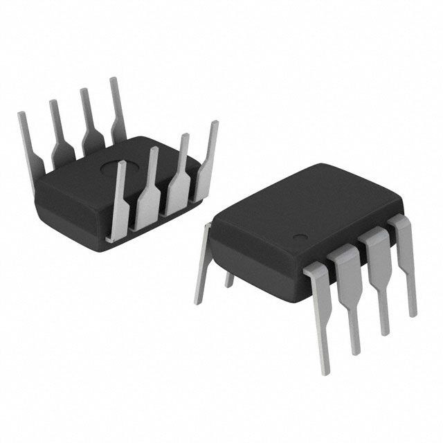
TLC2652ACP

Why Choose Us?
Professional Platform
B2B & B2C purchasingDelivery at full speed
1-2 days deliveryWide variety
Original manufacturers365 days guarantee
Responsible quality
.png)


Tech Specifications
TLC2652ACP Description
TLC2652ACP Description
The TLC2652ACP is a high-performance operational amplifier from Texas Instruments, part of the LinCMOS™ series. This IC is designed for precision applications requiring low input offset voltage and low input bias current. It features a zero-drift architecture, ensuring exceptional stability and accuracy over time and temperature variations. The TLC2652ACP operates from a supply voltage range of 3.8V to 16V, making it suitable for a wide range of power supply configurations. With a gain bandwidth product of 1.9 MHz and a slew rate of 3.1V/µs, it delivers high-speed performance while maintaining precision.
TLC2652ACP Features
- Zero-Drift Architecture: Ensures minimal offset voltage drift over time and temperature, providing consistent performance in precision applications.
- Low Input Offset Voltage: At 0.5 µV, the TLC2652ACP offers superior accuracy compared to traditional op-amps, making it ideal for high-precision signal conditioning.
- Low Input Bias Current: With an input bias current of just 4 pA, it minimizes the loading effect on sensitive sources, preserving signal integrity.
- Wide Supply Voltage Range: Operates from 3.8V to 16V, offering flexibility in power supply design and compatibility with various system architectures.
- High Gain Bandwidth Product: A 1.9 MHz gain bandwidth product ensures high-speed performance, suitable for applications requiring fast signal processing.
- High Slew Rate: A 3.1V/µs slew rate allows for rapid response to large signal changes, maintaining signal fidelity in dynamic environments.
- Low Supply Current: Consumes only 1.5mA of supply current, optimizing power efficiency without compromising performance.
- High Output Current: Capable of delivering up to 50 mA per channel, it can drive substantial loads directly, reducing the need for additional buffer stages.
- Through Hole Mounting: The through-hole package type ensures robust mechanical stability and ease of integration into various circuit boards.
- Compliance and Safety: The TLC2652ACP is REACH unaffected and RoHS3 compliant, ensuring environmental safety and regulatory compliance.
TLC2652ACP Applications
The TLC2652ACP is well-suited for a variety of applications where precision and high performance are critical. Its zero-drift architecture and low input offset voltage make it ideal for:
- Precision Signal Conditioning: Ideal for applications requiring high accuracy and low noise, such as sensor interfaces and instrumentation.
- Analog-to-Digital Conversion: Enhances the accuracy of ADCs by providing a stable and precise input signal.
- Active Filters: Its high gain bandwidth product and slew rate make it suitable for designing high-performance active filters.
- Transimpedance Amplifiers: The low input bias current and high output current capability make it an excellent choice for photodiode and other current-to-voltage conversion applications.
- Medical Equipment: Suitable for medical devices where precision and reliability are paramount, such as patient monitoring equipment and diagnostic instruments.
- Industrial Control Systems: Provides precise control and signal processing in industrial automation and control systems.
Conclusion of TLC2652ACP
The TLC2652ACP from Texas Instruments is a versatile and high-performance operational amplifier designed for precision applications. Its zero-drift architecture, low input offset voltage, and low input bias current make it stand out in the market. With a wide supply voltage range, high gain bandwidth product, and high slew rate, it offers excellent performance and flexibility. The TLC2652ACP is ideal for applications requiring high accuracy and reliability, such as precision signal conditioning, analog-to-digital conversion, and active filters. Its compliance with REACH and RoHS3 standards ensures environmental safety and regulatory compliance. Whether in medical equipment, industrial control systems, or other precision applications, the TLC2652ACP delivers exceptional performance and reliability.
FAQ
Not available to buy online? Want the lower wholesale price? Please Send RFQ to get best price, we will respond immediately


.png?x-oss-process=image/format,webp/resize,h_32)


