
 German
 Japanese
 Portuguese
 Korea
Korea
 Mexico
 Dutch
Dutch


Texas Instruments
TLC2652CP

Why Choose Us?
Professional Platform
B2B & B2C purchasingDelivery at full speed
1-2 days deliveryWide variety
Original manufacturers365 days guarantee
Responsible quality
.png)


Tech Specifications
TLC2652CP Description
TLC2652CP Description
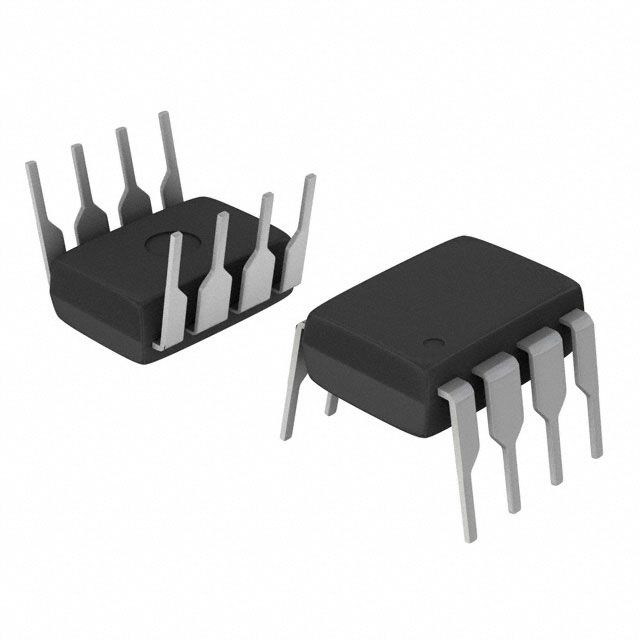
The TLC2652CP from Texas Instruments is a high-precision, zero-drift operational amplifier designed for applications requiring ultra-low input offset voltage and minimal drift over time. Part of the LinCMOS™ series, this IC integrates chopper-stabilization technology to achieve exceptional DC accuracy (0.6 µV input offset) and near-zero drift, making it ideal for precision signal conditioning. Operating over a 3.8V to 16V supply range, it delivers a 1.9 MHz gain bandwidth product and 3.1V/µs slew rate, balancing speed with low power consumption (1.5mA supply current). Housed in an 8-pin DIP through-hole package, it is suited for prototyping and industrial environments.
TLC2652CP Features
- Zero-Drift Architecture: Eliminates 1/f noise and offset drift, ensuring long-term stability.
- Ultra-Low Input Bias Current (4 pA): Minimizes errors in high-impedance sensor interfaces.
- Wide Supply Range (3.8V–16V): Compatible with single- or dual-supply designs.
- High Output Drive (50 mA): Capable of driving heavy loads directly.
- RoHS3 Compliant & REACH Unaffected: Meets environmental and regulatory standards.
- Extended Temperature Range (0°C to 70°C): Reliable performance in industrial settings.
TLC2652CP Applications
- Precision Instrumentation: Weigh scales, medical devices, and data acquisition systems benefit from its low noise and drift.
- Sensor Signal Conditioning: Ideal for thermocouples, RTDs, and bridge sensors due to µV-level accuracy.
- Active Filters & Integrators: The 1.9 MHz GBW supports low-distortion audio and control systems.
- Automotive & Industrial Controls: Robust performance in harsh environments with wide voltage tolerance.
Conclusion of TLC2652CP
The TLC2652CP stands out for its zero-drift precision, versatile supply range, and high output drive, addressing challenges in DC-sensitive applications. Its LinCMOS™ technology ensures reliability, while the through-hole package simplifies integration. For engineers seeking a balance of accuracy, speed, and power efficiency, this op-amp is a superior choice for high-end analog front-ends and low-frequency precision systems.
FAQ
Not available to buy online? Want the lower wholesale price? Please Send RFQ to get best price, we will respond immediately


.png?x-oss-process=image/format,webp/resize,h_32)


