
Texas Instruments
TLC272ACDR
OP Amps, Buffer Amps ICs


.png?x-oss-process=image/format,webp/resize,p_30)


TLC272ACDR Description
TLC272ACDR Description
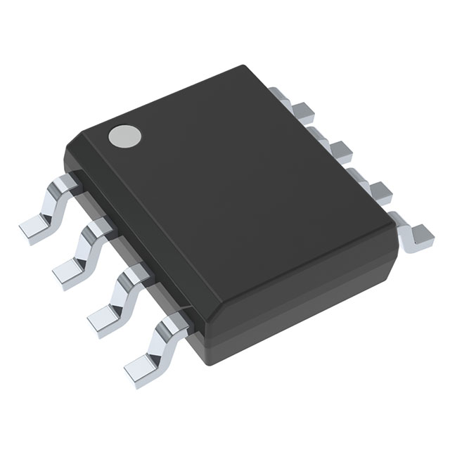
The TLC272ACDR is a high-performance, dual-channel, low-power operational amplifier (op-amp) from Texas Instruments. This CMOS op-amp is part of the LinCMOS™ series, designed for low-voltage, low-power applications. It operates over a wide supply voltage range of 3V to 16V and offers excellent DC performance with an input offset voltage of 900 µV and an input bias current of 0.7 pA. The device is available in an 8-SOIC package and is RoHS3 compliant, making it suitable for environmentally friendly designs.
TLC272ACDR Features
- Voltage - Supply Span (Max): 16V
- Voltage - Supply Span (Min): 3V
- Gain Bandwidth Product: 2.2 MHz
- Slew Rate: 5.3V/µs
- Current - Input Bias: 0.7 pA
- Current - Output / Channel: 30 mA
- Current - Supply: 1.9mA (x2 Channels)
- Voltage - Input Offset: 900 µV
- Operating Temperature: 0°C ~ 70°C (TA)
- Moisture Sensitivity Level (MSL): 1 (Unlimited)
- Mounting Type: Surface Mount
- Package: Tape & Reel (TR)
- Number of Circuits: 2
- Series: LinCMOS™
- Amplifier Type: CMOS
- Product Status: Active
- REACH Status: REACH Unaffected
- ECCN: EAR99
- HTSUS: 8542.33.0001
- RoHS Status: ROHS3 Compliant
TLC272ACDR Applications
The TLC272ACDR is ideal for a wide range of applications due to its low power consumption, low noise, and excellent DC performance. Some specific use cases include:
- Battery-powered devices: Its low power consumption makes it suitable for battery-powered applications, such as portable electronics and wearable devices.
- Sensor interfaces: The low input offset voltage and low input bias current make it an excellent choice for sensor interfaces, ensuring accurate signal processing.
- Audio applications: The low noise and high slew rate make it suitable for audio preamplifiers and other audio processing applications.
- Industrial control systems: The wide supply voltage range and high gain bandwidth product make it suitable for industrial control systems, where reliability and performance are critical.
Conclusion of TLC272ACDR
The TLC272ACDR is a versatile, low-power, dual-channel op-amp from Texas Instruments. Its unique combination of low power consumption, low noise, and excellent DC performance make it an ideal choice for a wide range of applications, including battery-powered devices, sensor interfaces, audio applications, and industrial control systems. With its RoHS3 compliance and wide supply voltage range, the TLC272ACDR is a reliable and environmentally friendly solution for your next design.
Tech Specifications
TLC272ACDR Documents
Download datasheets and manufacturer documentation for TLC272ACDR
 Assembly Site 22/Dec/2022
  TLC272/A/B/Y, TLC277
  Mult Devices Font 21/Apr/2018 Design 25/Feb/2022
 Shopping Guide


.png?x-oss-process=image/format,webp/resize,h_32)


