

Texas Instruments
TLC272AIP
OP Amps, Buffer Amps ICs

Not available to buy online? Want the lower wholesale price? Please Send RFQ to get best price, we will respond immediately


.png?x-oss-process=image/format,webp/resize,p_30)


TLC272AIP Description
TLC272AIP Description
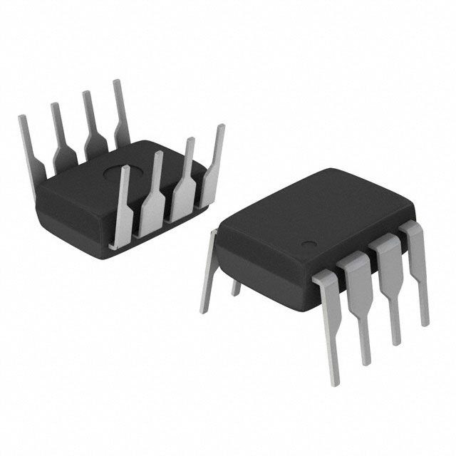
The TLC272AIP is a high-performance CMOS operational amplifier from Texas Instruments, designed to deliver exceptional performance in a wide range of applications. This dual-channel amplifier is part of the LinCMOS™ series, known for its low power consumption and excellent noise performance. The TLC272AIP is housed in a through-hole 8DIP package, making it suitable for both prototyping and production environments.
TLC272AIP Features
- Supply Voltage Range: The TLC272AIP operates over a wide supply voltage range of 4V to 16V, providing flexibility for various power supply configurations.
- Gain Bandwidth Product: With a gain bandwidth product of 2.2 MHz, this amplifier ensures high-frequency performance suitable for signal processing applications.
- Low Input Bias Current: The extremely low input bias current of 0.7 pA minimizes the impact of input bias on the signal, making it ideal for high-impedance circuits.
- High Slew Rate: The 5.3V/µs slew rate allows for rapid response to input signal changes, ensuring accurate reproduction of high-frequency signals.
- Low Input Offset Voltage: The 900 µV input offset voltage ensures minimal error in the output signal, enhancing the accuracy of the amplifier.
- Dual Channel Design: The TLC272AIP features two independent amplifier channels, each capable of sourcing 30 mA of output current, making it suitable for multi-signal processing tasks.
- Low Power Consumption: Consuming only 1.4mA per channel, this amplifier is highly efficient, reducing power dissipation and heat generation.
- Compliance and Reliability: The TLC272AIP is REACH unaffected and RoHS3 compliant, ensuring environmental safety and regulatory compliance. The moisture sensitivity level (MSL) is not applicable, further enhancing its reliability in various operating conditions.
TLC272AIP Applications
The TLC272AIP is ideal for a variety of applications due to its versatile performance characteristics. Some specific use cases include:
- Analog Signal Processing: The high gain bandwidth product and low input bias current make it suitable for applications requiring precise signal amplification and conditioning.
- Audio Applications: The low noise performance and high slew rate ensure high-fidelity audio signal processing, making it ideal for audio amplifiers and preamplifiers.
- Industrial Control Systems: The wide supply voltage range and robust performance make it suitable for industrial applications where reliability and precision are critical.
- Medical Equipment: The low input offset voltage and high accuracy make it suitable for medical devices where signal integrity is paramount.
Conclusion of TLC272AIP
The TLC272AIP from Texas Instruments is a versatile and high-performance CMOS operational amplifier that stands out in its category. Its wide supply voltage range, low power consumption, and excellent noise performance make it suitable for a wide range of applications. The dual-channel design and high slew rate further enhance its capabilities, making it an ideal choice for both analog signal processing and high-fidelity audio applications. The TLC272AIP's compliance with environmental and safety standards ensures its reliability and suitability for modern electronics design.
Tech Specifications
TLC272AIP Documents
Download datasheets and manufacturer documentation for TLC272AIP
TLC272/A/B/Y, TLC277 Copper Bond Wire Revision A 04/Dec/2013 Mult Dev 09/Jun/2023 Related Parts


Shopping Guide


.png?x-oss-process=image/format,webp/resize,h_32)


©2025 ERSA Electronics Corporation.